
Hi,
I cannot locate any QPI sample code in the example. Was it possible for anyone to share me the sample code?
Thanks a bunch.
Hi,
I cannot locate any QPI sample code in the example. Was it possible for anyone to share me the sample code?
Thanks a bunch.
Do you mean QSPI? If so: QSPI Example.
Hi haakonsh
Thanks for the quick feedback. But when I checked the solutions, I think QPI and Quad SPI is different solutions.
Quad SPI
While dual SPI re-uses the existing serial I/O lines, quad SPI adds two more I/O lines (SIO2 and SIO3) and sends 4 data bits per clock cycle. Again, it is requested by special commands, which enable quad mode after the command itself is sent in single mode.
SQI Type 1: Commands sent on single line but addresses and data sent on four lines
SQI Type 2: Commands and addresses sent on a single line but data sent/received on four lines
QPI/SQI
Further extending quad SPI, some devices support a "quad everything" mode where all communication takes place over 4 data lines, including commands.[19] This is variously called "QPI"[18] (not to be confused with Intel QuickPath Interconnect) or "serial quad I/O" (SQI)[20]
This requires programming a configuration bit in the device and requires care after reset to establish communication.
https://en.wikipedia.org/wiki/Serial_Peripheral_Interface#QPI/SQI
Thanks a bunch haakonsh, kindly refer to the attached link. Besides that, may I know how to support this chip using the quadspi sample? The reason I turn to QPI is because the quadspi sample just don't works with this chip.
http://www.cypress.com/file/316661/download
Model:S25FL064LABNFI010
Well, we should be able to interface with this memory chip via standard QSPI. Do you have a logic analyzer scope of the communication when using the SDK example?
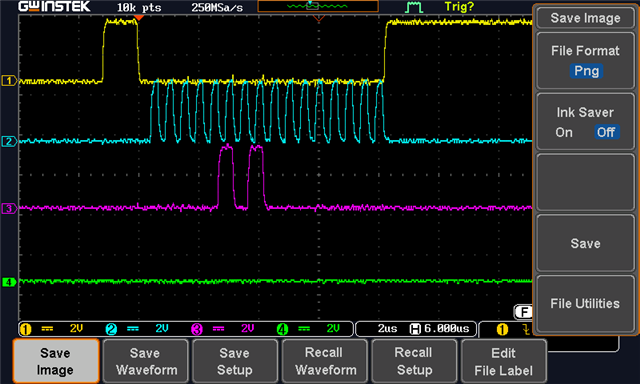
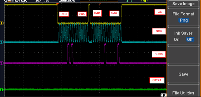
Will nrf_drv_qspi_init(&config, qspi_handler, NULL) trigger the SPI to sent out data? I notice my logic analyzer capture some data (0x500) when the nrf_drv_qspi_init is executed. I forget to add on, the yellow 1 is CS, blue 2 is SCK, purple 3 is SI/SI0 and green 4 on the scope is refer to SO/SI1
Here is the test configure code.
#define QSPI_STD_CMD_WRSR 0x01
#define QSPI_STD_CMD_RSTEN 0x66
#define QSPI_STD_CMD_RST 0x99
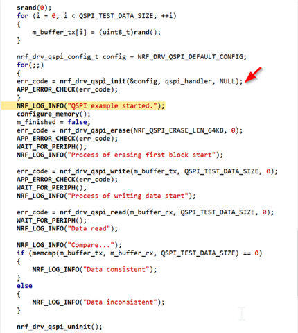
static void configure_memory()
{
uint8_t temporary[2] = {0x02,0x02};
uint32_t err_code;
nrf_qspi_cinstr_conf_t cinstr_cfg = {
.opcode = QSPI_STD_CMD_RSTEN,
.length = NRF_QSPI_CINSTR_LEN_1B,
.io2_level = true,
.io3_level = true,
.wipwait = true,
.wren = false
};
// Send reset enable
err_code = nrf_drv_qspi_cinstr_xfer(&cinstr_cfg, NULL, NULL);
APP_ERROR_CHECK(err_code);
// Send reset command
cinstr_cfg.opcode = QSPI_STD_CMD_RST;
err_code = nrf_drv_qspi_cinstr_xfer(&cinstr_cfg, NULL, NULL);
APP_ERROR_CHECK(err_code);
// Send WREN
cinstr_cfg.opcode = 0x71;
err_code = nrf_drv_qspi_cinstr_xfer(&cinstr_cfg, NULL, NULL);
APP_ERROR_CHECK(err_code);
// Switch to qspi mode
cinstr_cfg.opcode = QSPI_STD_CMD_WRSR;
cinstr_cfg.length = NRF_QSPI_CINSTR_LEN_2B;
err_code = nrf_drv_qspi_cinstr_xfer(&cinstr_cfg, &temporary, NULL);
APP_ERROR_CHECK(err_code);
}
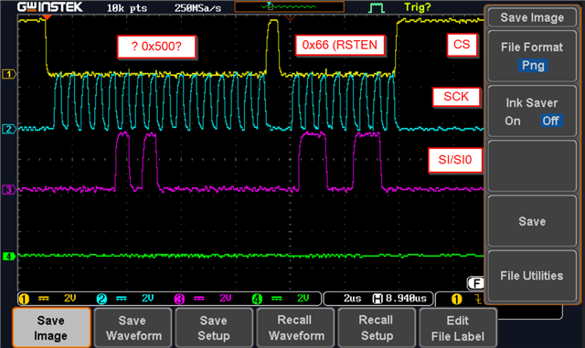
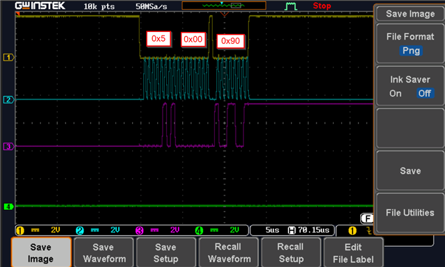
And I tried capture the reset enable command send when configure_memory function is called, the I notice there is extra data in front of the 0x66 command is that correct? What are those data for?
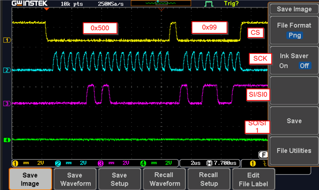
Here is the capture for RST command 0x99
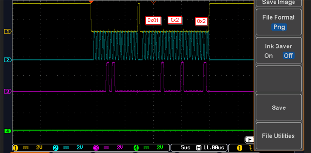
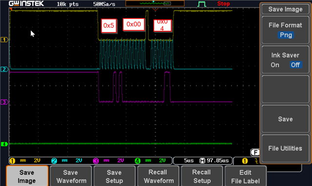
Here is the capture for WRAR command 0x06
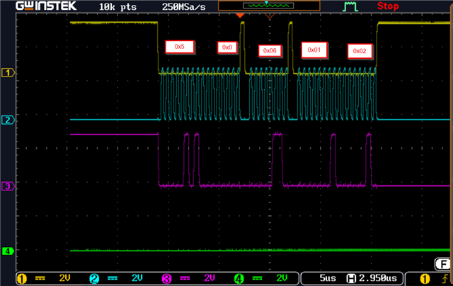
Here is the capture for WRR (0x01) + SR1NV (0x02) + CR1NV (0x02), it seem tgat CR1NV is not written
So I decided to modify the NRF_QSPI_CINSTR_LEN_2B to NRF_QSPI_CINSTR_LEN_3B
static void configure_memory()
{
    uint8_t temporary[2] = {0x02,0x02};
    uint32_t err_code;
    nrf_qspi_cinstr_conf_t cinstr_cfg = {
        .opcode    = QSPI_STD_CMD_RSTEN,
        .length    = NRF_QSPI_CINSTR_LEN_1B,
        .io2_level = true,
        .io3_level = true,
        .wipwait   = true,
        .wren      = false
    };

    // Send reset enable
    err_code = nrf_drv_qspi_cinstr_xfer(&cinstr_cfg, NULL, NULL);
    APP_ERROR_CHECK(err_code);

    // Send reset command
    cinstr_cfg.opcode = QSPI_STD_CMD_RST;
    err_code = nrf_drv_qspi_cinstr_xfer(&cinstr_cfg, NULL, NULL);
    APP_ERROR_CHECK(err_code);

    // Send WREN
    cinstr_cfg.opcode = 0X06;
    err_code = nrf_drv_qspi_cinstr_xfer(&cinstr_cfg, NULL, NULL);
    APP_ERROR_CHECK(err_code);

    // Switch to qspi mode
    cinstr_cfg.opcode = QSPI_STD_CMD_WRSR;
    cinstr_cfg.length = NRF_QSPI_CINSTR_LEN_3B;
    err_code = nrf_drv_qspi_cinstr_xfer(&cinstr_cfg, &temporary, NULL);
    APP_ERROR_CHECK(err_code);
}
The data output achieve what I wanted. But I not able to get any data reply from the memory chip
And sub-sequence I capture the nrf_drv_qspi_erase() data frame
Next, I decided to enable the .wren bit and hence it will added an extra 0x06 after the unknown data (0x5, 0x0) for all our configuration frame. Therefore I disable the WREN command, and I still not able to get a reply from the memory chip.  I suspect the unknown 0x5,0x00 data is the one affecting my memory, as I tried to read using normal spi mode, it fails. It only works when I replace the memory with flash memory chip.
static void configure_memory()
{
    uint8_t temporary[2] = {0x02,0x02};
    uint32_t err_code;
    nrf_qspi_cinstr_conf_t cinstr_cfg = {
        .opcode    = QSPI_STD_CMD_RSTEN,
        .length    = NRF_QSPI_CINSTR_LEN_1B,
        .io2_level = true,
        .io3_level = true,
        .wipwait   = true,
        .wren      = true
    };
    // Send reset enable
    err_code = nrf_drv_qspi_cinstr_xfer(&cinstr_cfg, NULL, NULL);
    APP_ERROR_CHECK(err_code);

    // Send reset command
    cinstr_cfg.opcode = QSPI_STD_CMD_RST;
    err_code = nrf_drv_qspi_cinstr_xfer(&cinstr_cfg, NULL, NULL);
    APP_ERROR_CHECK(err_code);

//    // Send WREN
//      cinstr_cfg.opcode = 0x06;
//    err_code = nrf_drv_qspi_cinstr_xfer(&cinstr_cfg, NULL, NULL);
//    APP_ERROR_CHECK(err_code);

    // Switch to qspi mode
    cinstr_cfg.opcode = QSPI_STD_CMD_WRSR;
    cinstr_cfg.length = NRF_QSPI_CINSTR_LEN_3B;
    err_code = nrf_drv_qspi_cinstr_xfer(&cinstr_cfg, &temporary, NULL);
    APP_ERROR_CHECK(err_code);
}My first thoughts are that those I/O lines are way too capacitively loaded. I need you to set the drive strength of the IO pins to NRF_GPIO_PIN_H0H1.
Thanks.
I tried the change the below code(under nrf_gpio.h), still no improvement. I was able to read the register using SPI master sample code from nordic nRF5_SDK_15.2.0_9412b96\examples\peripheral\spi
Do you know how can I use the qspi example(using nrf_drv_qspi_cinstr_xfer()) to read the register? I believe it will be great if I could at least test whether the register read is working before go into writing it.
__STATIC_INLINE void nrf_gpio_cfg_output(uint32_t pin_number)
{
    nrf_gpio_cfg(
        pin_number,
        NRF_GPIO_PIN_DIR_OUTPUT,
        NRF_GPIO_PIN_INPUT_DISCONNECT,
        NRF_GPIO_PIN_NOPULL,
//old        NRF_GPIO_PIN_S0S1,
		NRF_GPIO_PIN_H0H1,
        NRF_GPIO_PIN_NOSENSE);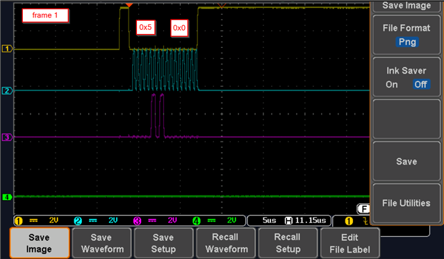
}And when I take a closer look into the timing diagram I captured.
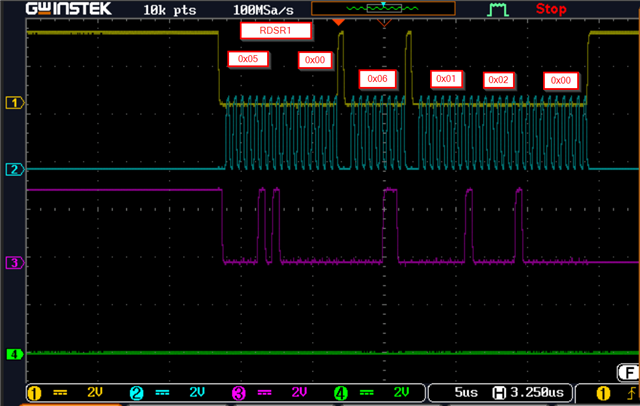
1) when using NRF_QSPI_CINSTR_LEN_2B, one frame is missing. We should have 0x5,0x00, 0x06(WREN), 0x01(WRSR), 0x02(SR1NV),0x02(CR1NV). But in fact, from the diagram I only get 0x5,0x00, 0x06(WREN), 0x01(WRSR), 0x02(SR1NV)
static void configure_memory()
{
    uint16_t setting_spec[2] = {0x02,0x02};
    uint32_t err_code;
    nrf_qspi_cinstr_conf_t cinstr_cfg = {
        .opcode    = QSPI_STD_CMD_RSTEN,
        .length    = NRF_QSPI_CINSTR_LEN_1B,
        .io2_level = true,
        .io3_level = true,
        .wipwait   = true,
        .wren      = true
    };
    // Send reset enable
    err_code = nrf_drv_qspi_cinstr_xfer(&cinstr_cfg, NULL, NULL);
    APP_ERROR_CHECK(err_code);

    // Send reset command
    cinstr_cfg.opcode = QSPI_STD_CMD_RST;
    err_code = nrf_drv_qspi_cinstr_xfer(&cinstr_cfg, NULL, NULL);
    APP_ERROR_CHECK(err_code);

    // Switch to qspi mode
    cinstr_cfg.opcode = 0x01;
    cinstr_cfg.length = NRF_QSPI_CINSTR_LEN_2B;
    err_code = nrf_drv_qspi_cinstr_xfer(&cinstr_cfg, setting_spec, NULL);
    APP_ERROR_CHECK(err_code);
}
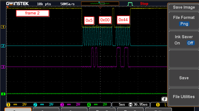
2) when using NRF_QSPI_CINSTR_LEN_3B, one frame is empty. We should have 0x5,0x00, 0x06(WREN), 0x01(WRSR), 0x02(SR1NV),0x02(CR1NV). But in fact, from the diagram I only get 0x5,0x00, 0x06(WREN), 0x01(WRSR), 0x02(SR1NV), 0x00(CR1NV) <---- missing data
static void configure_memory()
{
    uint16_t setting_spec[2] = {0x02,0x02};
    uint32_t err_code;
    nrf_qspi_cinstr_conf_t cinstr_cfg = {
        .opcode    = QSPI_STD_CMD_RSTEN,
        .length    = NRF_QSPI_CINSTR_LEN_1B,
        .io2_level = true,
        .io3_level = true,
        .wipwait   = true,
        .wren      = true
    };
    // Send reset enable
    err_code = nrf_drv_qspi_cinstr_xfer(&cinstr_cfg, NULL, NULL);
    APP_ERROR_CHECK(err_code);

    // Send reset command
    cinstr_cfg.opcode = QSPI_STD_CMD_RST;
    err_code = nrf_drv_qspi_cinstr_xfer(&cinstr_cfg, NULL, NULL);
    APP_ERROR_CHECK(err_code);

    // Switch to qspi mode
    cinstr_cfg.opcode = 0x01;
    cinstr_cfg.length = NRF_QSPI_CINSTR_LEN_3B;
    err_code = nrf_drv_qspi_cinstr_xfer(&cinstr_cfg, setting_spec, NULL);
    APP_ERROR_CHECK(err_code);
}
Maybe you need to use NRF_QSPI_CINSTR_LEN_2B

