Hi,
I cannot locate any QPI sample code in the example. Was it possible for anyone to share me the sample code?
Thanks a bunch.
Hi,
I cannot locate any QPI sample code in the example. Was it possible for anyone to share me the sample code?
Thanks a bunch.
Do you mean QSPI? If so: QSPI Example.
Hi haakonsh
Thanks for the quick feedback. But when I checked the solutions, I think QPI and Quad SPI is different solutions.
Quad SPI
While dual SPI re-uses the existing serial I/O lines, quad SPI adds two more I/O lines (SIO2 and SIO3) and sends 4 data bits per clock cycle. Again, it is requested by special commands, which enable quad mode after the command itself is sent in single mode.
SQI Type 1: Commands sent on single line but addresses and data sent on four lines
SQI Type 2: Commands and addresses sent on a single line but data sent/received on four lines
QPI/SQI
Further extending quad SPI, some devices support a "quad everything" mode where all communication takes place over 4 data lines, including commands.[19] This is variously called "QPI"[18] (not to be confused with Intel QuickPath Interconnect) or "serial quad I/O" (SQI)[20]
This requires programming a configuration bit in the device and requires care after reset to establish communication.
https://en.wikipedia.org/wiki/Serial_Peripheral_Interface#QPI/SQI
Next, I decided to enable the .wren bit and hence it will added an extra 0x06 after the unknown data (0x5, 0x0) for all our configuration frame. Therefore I disable the WREN command, and I still not able to get a reply from the memory chip. I suspect the unknown 0x5,0x00 data is the one affecting my memory, as I tried to read using normal spi mode, it fails. It only works when I replace the memory with flash memory chip.
static void configure_memory()
{
    uint8_t temporary[2] = {0x02,0x02};
    uint32_t err_code;
    nrf_qspi_cinstr_conf_t cinstr_cfg = {
        .opcode    = QSPI_STD_CMD_RSTEN,
        .length    = NRF_QSPI_CINSTR_LEN_1B,
        .io2_level = true,
        .io3_level = true,
        .wipwait   = true,
        .wren      = true
    };
    // Send reset enable
    err_code = nrf_drv_qspi_cinstr_xfer(&cinstr_cfg, NULL, NULL);
    APP_ERROR_CHECK(err_code);

    // Send reset command
    cinstr_cfg.opcode = QSPI_STD_CMD_RST;
    err_code = nrf_drv_qspi_cinstr_xfer(&cinstr_cfg, NULL, NULL);
    APP_ERROR_CHECK(err_code);

//    // Send WREN
//      cinstr_cfg.opcode = 0x06;
//    err_code = nrf_drv_qspi_cinstr_xfer(&cinstr_cfg, NULL, NULL);
//    APP_ERROR_CHECK(err_code);

    // Switch to qspi mode
    cinstr_cfg.opcode = QSPI_STD_CMD_WRSR;
    cinstr_cfg.length = NRF_QSPI_CINSTR_LEN_3B;
    err_code = nrf_drv_qspi_cinstr_xfer(&cinstr_cfg, &temporary, NULL);
    APP_ERROR_CHECK(err_code);
}My first thoughts are that those I/O lines are way too capacitively loaded. I need you to set the drive strength of the IO pins to NRF_GPIO_PIN_H0H1.
Thanks.
I tried the change the below code(under nrf_gpio.h), still no improvement. I was able to read the register using SPI master sample code from nordic nRF5_SDK_15.2.0_9412b96\examples\peripheral\spi
Do you know how can I use the qspi example(using nrf_drv_qspi_cinstr_xfer()) to read the register? I believe it will be great if I could at least test whether the register read is working before go into writing it.
__STATIC_INLINE void nrf_gpio_cfg_output(uint32_t pin_number)
{
    nrf_gpio_cfg(
        pin_number,
        NRF_GPIO_PIN_DIR_OUTPUT,
        NRF_GPIO_PIN_INPUT_DISCONNECT,
        NRF_GPIO_PIN_NOPULL,
//old        NRF_GPIO_PIN_S0S1,
		NRF_GPIO_PIN_H0H1,
        NRF_GPIO_PIN_NOSENSE);
}And when I take a closer look into the timing diagram I captured.
1) when using NRF_QSPI_CINSTR_LEN_2B, one frame is missing. We should have 0x5,0x00, 0x06(WREN), 0x01(WRSR), 0x02(SR1NV),0x02(CR1NV). But in fact, from the diagram I only get 0x5,0x00, 0x06(WREN), 0x01(WRSR), 0x02(SR1NV)
static void configure_memory()
{
    uint16_t setting_spec[2] = {0x02,0x02};
    uint32_t err_code;
    nrf_qspi_cinstr_conf_t cinstr_cfg = {
        .opcode    = QSPI_STD_CMD_RSTEN,
        .length    = NRF_QSPI_CINSTR_LEN_1B,
        .io2_level = true,
        .io3_level = true,
        .wipwait   = true,
        .wren      = true
    };
    // Send reset enable
    err_code = nrf_drv_qspi_cinstr_xfer(&cinstr_cfg, NULL, NULL);
    APP_ERROR_CHECK(err_code);

    // Send reset command
    cinstr_cfg.opcode = QSPI_STD_CMD_RST;
    err_code = nrf_drv_qspi_cinstr_xfer(&cinstr_cfg, NULL, NULL);
    APP_ERROR_CHECK(err_code);

    // Switch to qspi mode
    cinstr_cfg.opcode = 0x01;
    cinstr_cfg.length = NRF_QSPI_CINSTR_LEN_2B;
    err_code = nrf_drv_qspi_cinstr_xfer(&cinstr_cfg, setting_spec, NULL);
    APP_ERROR_CHECK(err_code);
}
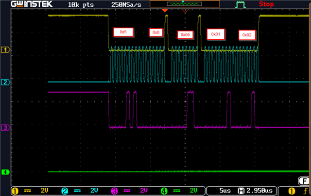
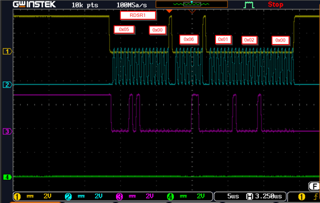
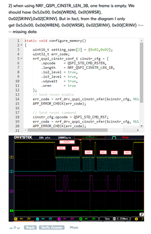
2) when using NRF_QSPI_CINSTR_LEN_3B, one frame is empty. We should have 0x5,0x00, 0x06(WREN), 0x01(WRSR), 0x02(SR1NV),0x02(CR1NV). But in fact, from the diagram I only get 0x5,0x00, 0x06(WREN), 0x01(WRSR), 0x02(SR1NV), 0x00(CR1NV) <---- missing data
static void configure_memory()
{
    uint16_t setting_spec[2] = {0x02,0x02};
    uint32_t err_code;
    nrf_qspi_cinstr_conf_t cinstr_cfg = {
        .opcode    = QSPI_STD_CMD_RSTEN,
        .length    = NRF_QSPI_CINSTR_LEN_1B,
        .io2_level = true,
        .io3_level = true,
        .wipwait   = true,
        .wren      = true
    };
    // Send reset enable
    err_code = nrf_drv_qspi_cinstr_xfer(&cinstr_cfg, NULL, NULL);
    APP_ERROR_CHECK(err_code);

    // Send reset command
    cinstr_cfg.opcode = QSPI_STD_CMD_RST;
    err_code = nrf_drv_qspi_cinstr_xfer(&cinstr_cfg, NULL, NULL);
    APP_ERROR_CHECK(err_code);

    // Switch to qspi mode
    cinstr_cfg.opcode = 0x01;
    cinstr_cfg.length = NRF_QSPI_CINSTR_LEN_3B;
    err_code = nrf_drv_qspi_cinstr_xfer(&cinstr_cfg, setting_spec, NULL);
    APP_ERROR_CHECK(err_code);
}
Maybe you need to use NRF_QSPI_CINSTR_LEN_2B
Maybe you need to use NRF_QSPI_CINSTR_LEN_2B
hI haakonsh
Thanks for the suggestion.
If I use NRF_QSPI_CINSTR_LEN_2B, I will only have one data sent out for example, my string is 0x02,0x02. It will sent out 0x02 only. Its already shown in my previous post.
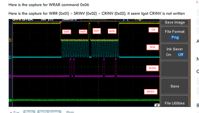
Ahh my bad I think the length config should be NRF_QSPI_CINSTR_LEN_3B when you've got 2 data bytes in your custom commands
Hi haakonsh
Thanks. I have tried NRF_QSPI_CINSTR_LEN_3B but I notice the output of the last byte is 0x00 rather than 0x02. Please advice is this a bug?
Ahh, sorry I missed that.
I believe the reason that you get 0x02, 0x00 is that you declared the buffer as uint16_t whereas the QSPI operates on bytes.
ie:
NRF_QSPI_CINSTR_LEN_5B should yield 0x02, 0x00, 0x02, 0x00.
Thanks @haakonsh,
I would like to learn to understand and how to configure prot_if parameters.
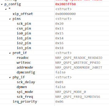
readoc structure
1) NRF_QSPI_READOC_READ4IO = 0xEB which is Quad I/O Read which is same as S25F064L Quad I/O Read 0xEB?
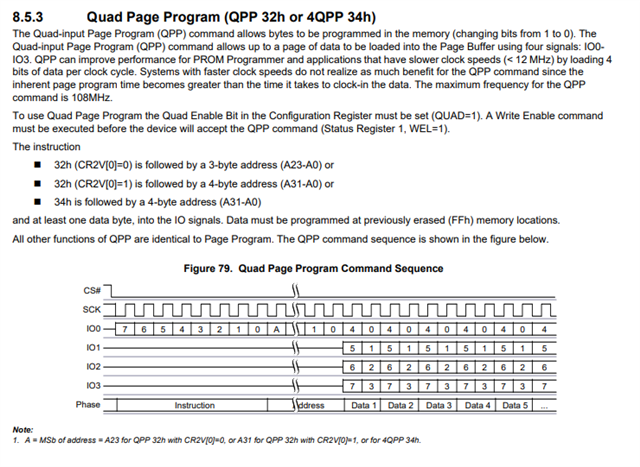
2) NRF_QSPI_WRITEOC_PP4IO = 0x38 for MX25R6435F chip its 4PP? Was it the same as S25F064L 4QPP which is 0x34?
If I want to change those value, where can I change it? I just don't understand the code in nrf52840_bitfields.h, and how can I change if the PP4IO instruction if its different?
/* Bits 5..3 : Configure number of data lines and opcode used for writing. */
#define QSPI_IFCONFIG0_WRITEOC_Pos (3UL) /*!< Position of WRITEOC field. */
#define QSPI_IFCONFIG0_WRITEOC_Msk (0x7UL << QSPI_IFCONFIG0_WRITEOC_Pos) /*!< Bit mask of WRITEOC field. */
#define QSPI_IFCONFIG0_WRITEOC_PP (0UL) /*!< Single data line SPI. PP (opcode 0x02). */
#define QSPI_IFCONFIG0_WRITEOC_PP2O (1UL) /*!< Dual data line SPI. PP2O (opcode 0xA2). */
#define QSPI_IFCONFIG0_WRITEOC_PP4O (2UL) /*!< Quad data line SPI. PP4O (opcode 0x32). */
#define QSPI_IFCONFIG0_WRITEOC_PP4IO (3UL) /*!< Quad data line SPI. PP4IO (opcode 0x38). */
3) The S25F064L chip come in SPI as default setting, is the on board PCA10056 DK MX25R6435F already preconfigured with QSPI setting? If yes, How can I the command in SPI using QSPI resource?
4) is the default QSPI sample setting same for operation below?
