Hi,
I cannot locate any QPI sample code in the example. Was it possible for anyone to share me the sample code?
Thanks a bunch.
Hi,
I cannot locate any QPI sample code in the example. Was it possible for anyone to share me the sample code?
Thanks a bunch.
Do you mean QSPI? If so: QSPI Example.
Hi haakonsh
Thanks for the quick feedback. But when I checked the solutions, I think QPI and Quad SPI is different solutions.
Quad SPI
While dual SPI re-uses the existing serial I/O lines, quad SPI adds two more I/O lines (SIO2 and SIO3) and sends 4 data bits per clock cycle. Again, it is requested by special commands, which enable quad mode after the command itself is sent in single mode.
SQI Type 1: Commands sent on single line but addresses and data sent on four lines
SQI Type 2: Commands and addresses sent on a single line but data sent/received on four lines
QPI/SQI
Further extending quad SPI, some devices support a "quad everything" mode where all communication takes place over 4 data lines, including commands.[19] This is variously called "QPI"[18] (not to be confused with Intel QuickPath Interconnect) or "serial quad I/O" (SQI)[20]
This requires programming a configuration bit in the device and requires care after reset to establish communication.
https://en.wikipedia.org/wiki/Serial_Peripheral_Interface#QPI/SQI
And when I take a closer look into the timing diagram I captured.
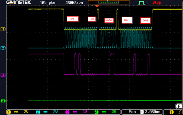
1) when using NRF_QSPI_CINSTR_LEN_2B, one frame is missing. We should have 0x5,0x00, 0x06(WREN), 0x01(WRSR), 0x02(SR1NV),0x02(CR1NV). But in fact, from the diagram I only get 0x5,0x00, 0x06(WREN), 0x01(WRSR), 0x02(SR1NV)
static void configure_memory()
{
    uint16_t setting_spec[2] = {0x02,0x02};
    uint32_t err_code;
    nrf_qspi_cinstr_conf_t cinstr_cfg = {
        .opcode    = QSPI_STD_CMD_RSTEN,
        .length    = NRF_QSPI_CINSTR_LEN_1B,
        .io2_level = true,
        .io3_level = true,
        .wipwait   = true,
        .wren      = true
    };
    // Send reset enable
    err_code = nrf_drv_qspi_cinstr_xfer(&cinstr_cfg, NULL, NULL);
    APP_ERROR_CHECK(err_code);

    // Send reset command
    cinstr_cfg.opcode = QSPI_STD_CMD_RST;
    err_code = nrf_drv_qspi_cinstr_xfer(&cinstr_cfg, NULL, NULL);
    APP_ERROR_CHECK(err_code);

    // Switch to qspi mode
    cinstr_cfg.opcode = 0x01;
    cinstr_cfg.length = NRF_QSPI_CINSTR_LEN_2B;
    err_code = nrf_drv_qspi_cinstr_xfer(&cinstr_cfg, setting_spec, NULL);
    APP_ERROR_CHECK(err_code);
}
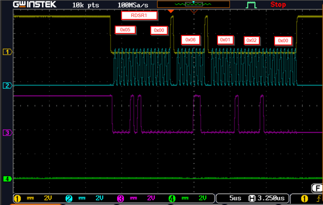
2) when using NRF_QSPI_CINSTR_LEN_3B, one frame is empty. We should have 0x5,0x00, 0x06(WREN), 0x01(WRSR), 0x02(SR1NV),0x02(CR1NV). But in fact, from the diagram I only get 0x5,0x00, 0x06(WREN), 0x01(WRSR), 0x02(SR1NV), 0x00(CR1NV) <---- missing data
static void configure_memory()
{
    uint16_t setting_spec[2] = {0x02,0x02};
    uint32_t err_code;
    nrf_qspi_cinstr_conf_t cinstr_cfg = {
        .opcode    = QSPI_STD_CMD_RSTEN,
        .length    = NRF_QSPI_CINSTR_LEN_1B,
        .io2_level = true,
        .io3_level = true,
        .wipwait   = true,
        .wren      = true
    };
    // Send reset enable
    err_code = nrf_drv_qspi_cinstr_xfer(&cinstr_cfg, NULL, NULL);
    APP_ERROR_CHECK(err_code);

    // Send reset command
    cinstr_cfg.opcode = QSPI_STD_CMD_RST;
    err_code = nrf_drv_qspi_cinstr_xfer(&cinstr_cfg, NULL, NULL);
    APP_ERROR_CHECK(err_code);

    // Switch to qspi mode
    cinstr_cfg.opcode = 0x01;
    cinstr_cfg.length = NRF_QSPI_CINSTR_LEN_3B;
    err_code = nrf_drv_qspi_cinstr_xfer(&cinstr_cfg, setting_spec, NULL);
    APP_ERROR_CHECK(err_code);
}
Maybe you need to use NRF_QSPI_CINSTR_LEN_2B
hI haakonsh
Thanks for the suggestion.
If I use NRF_QSPI_CINSTR_LEN_2B, I will only have one data sent out for example, my string is 0x02,0x02. It will sent out 0x02 only. Its already shown in my previous post.
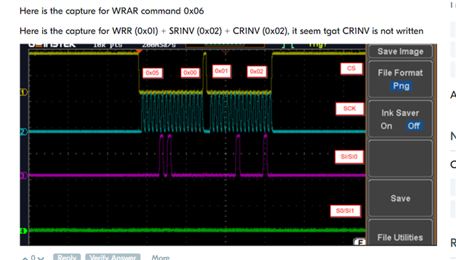
Ahh my bad I think the length config should be NRF_QSPI_CINSTR_LEN_3B when you've got 2 data bytes in your custom commands
Hi haakonsh
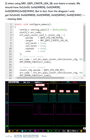
Thanks. I have tried NRF_QSPI_CINSTR_LEN_3B but I notice the output of the last byte is 0x00 rather than 0x02. Please advice is this a bug?
Hi haakonsh
Thanks. I have tried NRF_QSPI_CINSTR_LEN_3B but I notice the output of the last byte is 0x00 rather than 0x02. Please advice is this a bug?

Ahh, sorry I missed that.
I believe the reason that you get 0x02, 0x00 is that you declared the buffer as uint16_t whereas the QSPI operates on bytes.
ie:
NRF_QSPI_CINSTR_LEN_5B should yield 0x02, 0x00, 0x02, 0x00.
Thanks @haakonsh,
I would like to learn to understand and how to configure prot_if parameters.
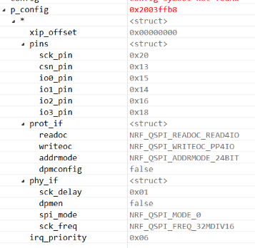
readoc structure
1) NRF_QSPI_READOC_READ4IO = 0xEB which is Quad I/O Read which is same as S25F064L Quad I/O Read 0xEB?
2) NRF_QSPI_WRITEOC_PP4IO = 0x38 for MX25R6435F chip its 4PP? Was it the same as S25F064L 4QPP which is 0x34?
If I want to change those value, where can I change it? I just don't understand the code in nrf52840_bitfields.h, and how can I change if the PP4IO instruction if its different?
/* Bits 5..3 : Configure number of data lines and opcode used for writing. */
#define QSPI_IFCONFIG0_WRITEOC_Pos (3UL) /*!< Position of WRITEOC field. */
#define QSPI_IFCONFIG0_WRITEOC_Msk (0x7UL << QSPI_IFCONFIG0_WRITEOC_Pos) /*!< Bit mask of WRITEOC field. */
#define QSPI_IFCONFIG0_WRITEOC_PP (0UL) /*!< Single data line SPI. PP (opcode 0x02). */
#define QSPI_IFCONFIG0_WRITEOC_PP2O (1UL) /*!< Dual data line SPI. PP2O (opcode 0xA2). */
#define QSPI_IFCONFIG0_WRITEOC_PP4O (2UL) /*!< Quad data line SPI. PP4O (opcode 0x32). */
#define QSPI_IFCONFIG0_WRITEOC_PP4IO (3UL) /*!< Quad data line SPI. PP4IO (opcode 0x38). */
3) The S25F064L chip come in SPI as default setting, is the on board PCA10056 DK MX25R6435F already preconfigured with QSPI setting? If yes, How can I the command in SPI using QSPI resource?
4) is the default QSPI sample setting same for operation below?
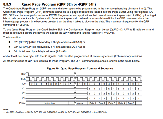
Hi,
I'm sorry for the delayed response. Haakon is currently out of office on business travel. Have you been able to solve this, or do you still need help?
Yes. I need help. The question will be as per the last question I asked, which is how to customize the QSPI sample code to enable QSPI in cypress Model:S25FL064LABNFI010
Hi, I have ordered the IC (S25FL064LABNFI010) so I can test it on my side. Should have it by Wednesday/Thursday this week. I'm going to study the datasheet in the meantime.