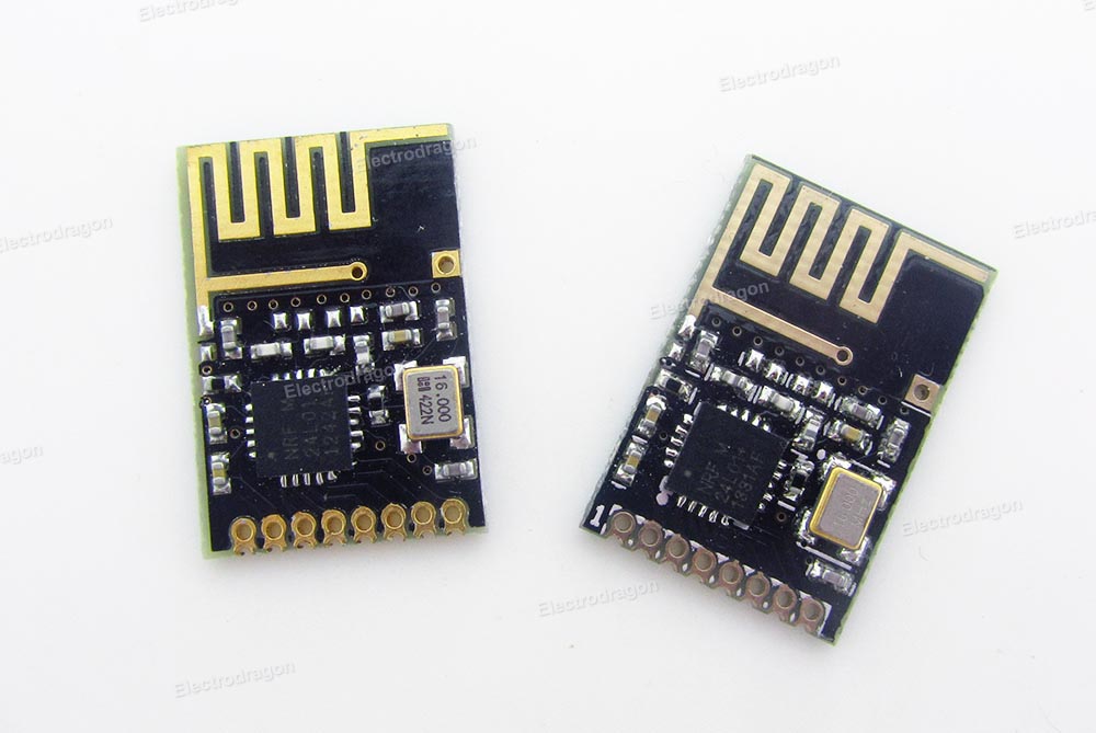
Hello guys,
I tried to design a pcb antenna for a nrf24l01+, since my company doesnt allow to buy cheap smd breakout board version from china anymore
The pcb stats of the producer:
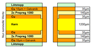
- 2-layer FR4 1.55mm (61.023mil) thickness, εr = 4.6
- Copper thickness, 35μm (1.378mil)
What I used:
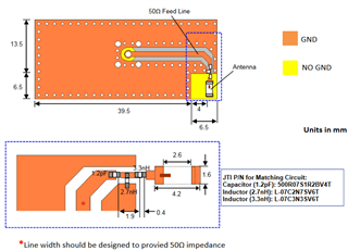
- Guideline for pcb mifa antenna design:https://www.cypress.com/file/136236/download :
Antenna basic dimensions: Page 10
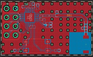
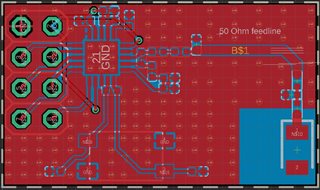
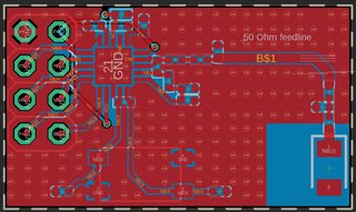
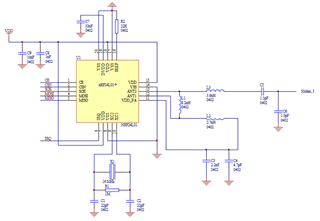
Cutting antenna length to ~115mil as told on page 14 - nrf24l01+ schematic pictured in the datasheet page 66 (rev1.0)
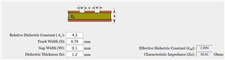
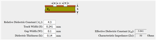
- https://www.eeweb.com/tools/microstrip-impedance for calculation resulting into a feedingline width of 2.82mm (111.023mil), this is double the value of the recommended value in the cypress file. Not sure whats right.
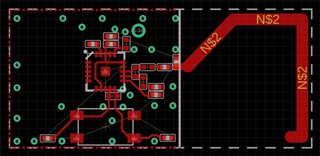
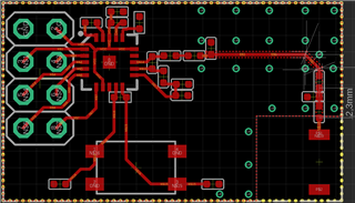
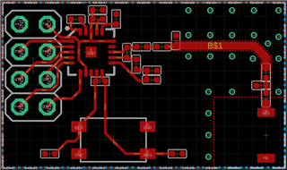
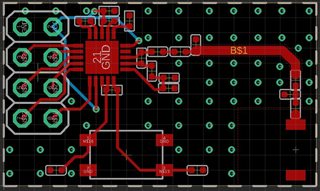
This results into following desgin block:
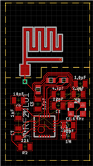
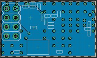
The antenna area is clear of any signals aswell as ground on top or bottom layer.
Since I have absolutly zero experience with RF antenna design I would like to have some opinions regarding my design.
Thanks so far,
Joe