This post is older than 2 years and might not be relevant anymore
More Info: Consider searching for newer posts

External Programming of a BL651 dev board using nRF52 DK

Hi,

I have recently developed a simple custom board with the use of the BL651 module to have a dev board for myself. Although the schematic diagram is simple and the PCB does not have any issues of incorrect soldering, I was not able to detect the BL651 module over the nrf52 DK using either P20 or P19 headers.

I have already gone through most of the previous posts with issues of programming externally with the nrf52 DK and if the connections are correct between the 2 boards, but I was still not succesful in detecting the nrf52810 of the BL651.

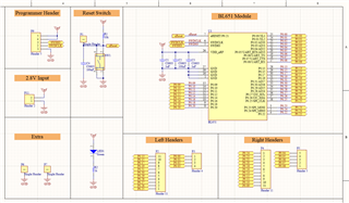
As such I checked the signals from the SWD IO and SWD CLKfrom the nrf52 DK and was not able to detect any changes in the voltage levels using an oscilloscope. For reference, here is the schematic I designed maybe there is something I missed.

Note that this is m first time using the Nordic Enviroment, where I am using the Segger EMbedded Studio for development and the nRF Connect, nRF GO Studio and the nrfjprog commands to try and detect the custom device.

Do you have any suggestion as to why I am not able to detect the BL651 IC and why does the nRF52 DK does not output any signals on the SWD IO and SWD CLK, as I have been stuck on this problem for 2 weeks as of now.

Thank you.
Parents
  • I would recommend posting the exact connections in the two cases which you tried; both to P19 and to P20. Particularly important are the Gnd and Vcc connections, and how vnrf is derived on the 2.8v input connector but we need to see all of the connections to be able to diagnose.

  • 2.8V was provided with both the nrf52 DK and also tested using an external voltage supply, using the P11 header in my schematic. 

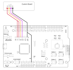
    The connection between the board with respect to the P20 of the DK was done as follows.

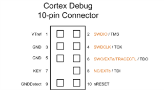
    For the P19 I had an Atmel ICE adaptor board to connect the 10-pin 1.27mm cable from which I mapped the connections and checked them through a multimeter, and the 10-pin connector (P19) was based to have the following connections for a typical Cortex JTAG/SWD Pinout. I still have to retest, but I am fairly certain the remapping is correct.


    However, with respect to the schematic in the main thread, did you find any inconsistencies in the connections for the BL651?

  • This is what I use on target boards using modules which have both the 10-way .05" pitch connector (same as P19) and a Tag-Connect 6-pin connector:

    10-Pin Cortex Debug Connector to 6-Pin TC2030 Footprint
    =======================================================
    1 VCC Sense     1
    3 GND           5
    5 GND           5
    7 NC / RTCK     -
    9 GND Detect    5
    2 SWDIO / TMS   2
    4 SWCLK / TCK   4
    6 SWO / TDO     6
    8 NC / TDI      -
    10 nRESET       3

    The target boards have the connection from the 10-way header as described above (all of them, no missing Gnd for example). I use a simple 10-way ribbon between nRF52DK P19 and the target board header.

    The 6-pin Tag-Connect is defined as this, which also works using the 6-pin to 20-pin J-TAG adapter board::

    1 VCC
    2 SWDIO / TMS
    3 nRESET
    4 SWCLK / TCK
    5 GND (also connected to GNDDetect)
    6 SWO / TDO

    P19 description and circuit diagram are shown in the nRF52DK User Manual:

    nRF52_DK_User_Guide_v1.2.pdf

  • The only difference I have from your connection is that the nReset and SWO pins are not connected from the P19 to the module. Would that do any difference, as they are not specified to be required for programming the device.

    In fact, I have just added those connections to the programmer too, but thus far was not able to detect the IC using either the Go Studio or the command nrfjprog -i.

  • nReset and SWO are not required. Your diagram does not show a connection to P19 pin 9; the connection from P20 pin 8 should be moved to P19 pin 9 as they are different functions (as I mentioned earlier). If you have already done that, maybe a Nordic engineer can shed some light. It is just possible it is a nRF52810-only issue which I am not aware of.

  • Sorry for the late message.

    I already had the connection when I tested the P19 header for pin 9, however it still did not do trick. I soldered a second board and got the same issue, which means that there is something wrong either with my connections which I am currently in the process of revising them or I am missing some form of initial configuration that I must first do.

    I also used the J-link commander to check the SWD connections by switching between the target device of NRF52810_XXAA and NRF52832_XXAA and got the same ID representing the nRF52 DK board.

  • Hi,

    Based on this discussion and the drawing from this post it seems that you have connected the debug interface correctly. In what way do things fail when you try to program/debug the external board with this setup?

    Braino said:
    I also used the J-link commander to check the SWD connections by switching between the target device of NRF52810_XXAA and NRF52832_XXAA and got the same ID representing the nRF52 DK board.

    You will always get the ID representing the nRF52 DK board since this is the ID of the onboard debugger. So it will be the same regardless of if you are debugging the onboard nRF or an external nRF via the debug out port.

Reply
  • Hi,

    Based on this discussion and the drawing from this post it seems that you have connected the debug interface correctly. In what way do things fail when you try to program/debug the external board with this setup?

    Braino said:
    I also used the J-link commander to check the SWD connections by switching between the target device of NRF52810_XXAA and NRF52832_XXAA and got the same ID representing the nRF52 DK board.

    You will always get the ID representing the nRF52 DK board since this is the ID of the onboard debugger. So it will be the same regardless of if you are debugging the onboard nRF or an external nRF via the debug out port.

Children
  • Hi,

    My issue is that when I was trying to program using the SES and changing the respective parameters such as to be able to program the BL651 module, I did not get a response. I tested it using simple LED and Bluetooth projects however none of them worked, but instead where being uploaded to the onboard nRF52832 IC of the dev kit.

    I also tried to get the respective information on the SWD interface using nrfjprog -i command, from which I understood that it should retrieve all the connected devices over the SWD interface. Are there further tests that I may be able to do to validate the connection?

    Also with respect to actual power I calculated roughly 2mA being drawn from the BL651 module which indicates that there is power delivered.

    I followed these guides, in addition to the datasheet.

    1.

    https://infocenter.nordicsemi.com/index.jsp?topic=%2Fcom.nordic.infocenter.sdk5.v15.3.0%2Fsdk_for_custom_boards.html&resultof=%22%63%75%73%74%6f%6d%22%20%22%62%6f%61%72%64%22%20
    2. 
    https://infocenter.nordicsemi.com/index.jsp?topic=%2Fcom.nordic.infocenter.sdk5.v15.3.0%2Fsdk_for_custom_boards.html&resultof=%22%63%75%73%74%6f%6d%22%20%22%62%6f%61%72%64%22%20

    What I was confused of was the definitions for the RAM and flash size parameters in SES when converting from PCA10040 to nRF52810 (BL651). Would you be able to provide a more in depth configuration procedure, maybe I have a missing step?

  • Hi, 

    Braino said:
    I tested it using simple LED and Bluetooth projects however none of them worked, but instead where being uploaded to the onboard nRF52832 IC of the dev kit.

    I see. It is perhaps a stupid question, but since I don't see any issue in the setup, can you just verify that GND detect is properly shorted to GND? That is how the onboard debugger decides if it should interface the onboard nRF or use the debut out port.

    Braino said:
    I also tried to get the respective information on the SWD interface using nrfjprog -i command, from which I understood that it should retrieve all the connected devices over the SWD interface.

    That is not the case. nrfjprog -i will print the ID of all connected Segger J-Link debuggers. So you will see the same ID regardless of which nRF52 chip the debugger is interfacing.

    Braino said:
    Are there further tests that I may be able to do to validate the connection?

    You could read out the value of a register that is unique for each chip, for instance, DEVICEID. As long as the value is the same you know you are debugging the same chip. If it differs, then you know you are debugging a different chip. Use for instance "nrfjprog.exe --memrd 0x10000060 --n 8".

    Braino said:
    What I was confused of was the definitions for the RAM and flash size parameters in SES when converting from PCA10040 to nRF52810 (BL651). Would you be able to provide a more in depth configuration procedure, maybe I have a missing step?

    If you are only adapting an existing example to a different chip, then the only linker related change is to adjust FLASH_SIZE and RAM_SIZE to reflect the new sizes (the sum of start address and size must not be larger than the physical flash). (If you are using a bootloader etc. that complicates a bit since you need to make room for that as well). See the image below for wher you configure this in SES.

    This is not related to the original question in this thread in itself, so I suggest you create a new question if you need to look more into this later.

  • Hi,

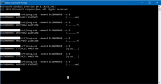
    Thank you for the quick response. Using the command you proposed I was able to retrieve the different device IDs of the 2 custom board I soldered. The issue was that I was using the wrong set of commands to validate the connections. The respective result is show below, where A01CA2C3 ... is from the dev kit, where as the other 2 are the custom boards.

    So from the point of connecting to the modules I am assuming it was successful since I obtained 3 different IDs. As such the remaining point which I need to revisit is why it is not successfully program, and from the last point you mentioned that I would need to take care of any internal boot-loader, where the BL651 modules do not advert any form of pre-configured loader.

    As you suggested, if I do not manage I will create a new thread for that and mark this as answered.

    Thank you for your time,
    Cheers Braino

Related