This post is older than 2 years and might not be relevant anymore
More Info: Consider searching for newer posts

Review request for a stacking PCB

Hello,

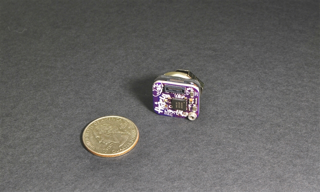
I'm trying to develop a wearable stacking form-factor where number of boards can be assembled in a deck: MCU, sensors, actuators, power supplies, etc. Size of the boards (cards) is kind of important for wearables, so for the proof of concept I've started with a tiny 20x20 mm PCB and nRF52832 QFN48, samples of which were included into DK and PPK (thanks!).

May I ask you to review the preliminary design of the board prototype, please?

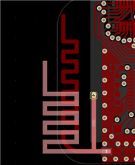
The board has 4 layers, 1.6 mm thick.

Antenna

Of course, the most challenging part is the RF. For such a small PCB with number of other boards beneath it I don't expect it performing high, but there're seem not too many options. I've had a chance to evaluate the Johanson 2450AT42E010BE zero clearance antenna on the board of about the same size (the rayBeacon), and it works. With tiny PCB footprint it looks like a clear winner among other possible options. On the dark side, it's tricky to tune and still suffer from narrow band due to very little ground area.

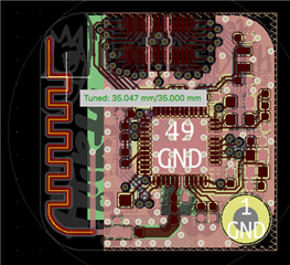
For the first prototype it might be reasonable to start with a printed antenna which I could tune by myself. One option is a monopole trace like that one on the nRF51 smart beacon. However, I've decided to go the harder way and adopted the well known MIFA. As far as I understood how it works, the inductance part of the F antenna is conveniently fixed parallel to the ground plane and seem requires no tuning, and the meandered trace can be easily cut to match the impedance. It's length is 35mm as shown on the picture below. Please also note, there is also one series component.

The antenna questions:

  1. Which one of the three is better - zero clearance chip antenna, monopole trace, the MIFA? Please note, the chip antenna means substantially bigger ground plane.
  2. Any advantages to keep the series component for the trace antenna, or can it be safely dropped?
  3. Should the board size of 20x20 mm be considered as too small for the radio? How much will it help if the board size will be increased to 24x24 mm?
  4. The very end of the meandered trace miss the complimentary ground plane on the top side. Is it an issue?

Of course, any other notes will be appreciated.
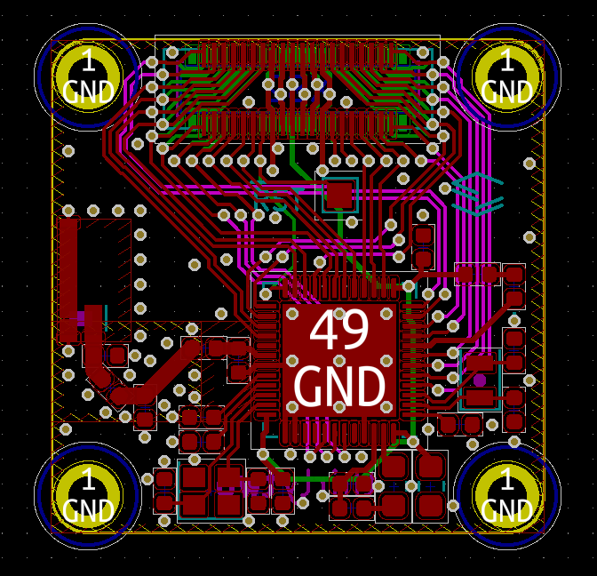
Other traces

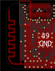
On the north of the board there are the two Hirose DF40 connectors. Placed on the top and on the bottom sides and linked each other, they're used to attach series of similar boards into a deck and act like a bus. Here is the pinout:

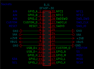
First concern is the NFC. The NFC traces are routed to the pins 29 and 30. Main idea about them is to have a dedicated board for the antenna. It was also planned to put tuning capacitors to the antenna board too. Unfortunately, the traces are walking over SWD traces, in particular SWDCLK and SWDIO. Passing NFC from board to board is also not the best idea either. But what do you think?

Another question is about the pins 40 to 43. Accordingly to the board design the pins must be reserved for SPI. But per section 4.3 GPIO Usage Restrictions they must be low frequency I/O. The nRF52832 doesn't support high-speed SPI, but should I be concerned about using the pins for 8MHz SPI?

Generally speaking, I'm not too happy about the "beard" from those vias around the DF40 - just trying to avoid HDI and keep fabrication cost low. Maybe there is something that I've missed about the connectors, and which terribly breaks the design?

I've attached design files. The silklayer is useless, but the *Fab files have all components and values referenced.

Thank you!

Mishka

rasytack-thirtytwo.zip

Parents
  • Hi,


    1. Generally PCB antennas are better. Meandered designs can be tricky to implement without proper tools unless it is a proven design, so often recommended to keep it simple. On-ground antennas should be avoided unless ground/metal underneath the antenna can not be avoided.
    2. Advantage is you do not need to spin the PCB in case it is needed for tuning the antenna. If not needed it can be shorted.
    3. Not too small, but probably small enough that RF performance will not be superb. Hard to say how much incresing to 24x24mm would improve, would expect some increase.
    4. Sorry, I do not understand what you mean.


    NFC: Passing to another board should not be a problem. Passing the traces over the SWD traces might not be optimal, but hard to say. If you want to be on the safe side you should separate them with ground in the internal layer(s).

    High-frequency IOs: High drive IOs and frequency >100kHz should be avoided during radio activity, some radio performance parametres can be affected.


    The connector I guess is what it is, but should not be too critical with regards to any performance from what I can see. Maybe it will be easier to get a more tidy design ig you move it slightly or extend the board slightly towards the north so that you can partly approach it from the other side? 


    Best regards,

    Andreas

  • Hi Andreas,

    thanks a lot for the helpful review!

    A couple of words regarding the MIFA. It's custom indeed, and I'm totally unsure would it work or not. Please take a look to a simple visual comparison of the MIFA and the reference antenna. I've tried to model it with the cocoaNEC, but failed to learn the language Disappointed

    In the question #4 about the very end of the meandered arm, I meant the area outlined on the screenshot below. The concern here is that the board misses top ground plane there which might affect radio performance.

    If switch to a monopole antenna, it might be possible to expand the top ground and align it with the bottom (gray on the screenshots above). Such, on the following screenshot there is a possible solution. The monopole length is about 24 mm as measured from the ground plane at the feed point and to the end. Trace width is 1.5 mm. I've dropped the serial component and the shunt capacitor is highlighted.

    How do you think, is it any better than the custom MIFA?

    About the need for a zero-clearance antenna, the board thickness is 1.6mm, minimal mated height for the DF40 connector is 1.5mm. Therefore for a typical case it's safe to assume there will be at least 3.1 mm clearance from a conventional antenna to bottom ground plane (which is actually the top ground plane of the bottom board). Is it possible at this stage to say which one is better / worse? Or is it required to assemble both and compare?

    Regarding the NFC and the high-freq IO: thanks for the advice! I'll try to move SPI to different pins, and also route SWD on the third plane. The SWD will collide with VDD in this case, but on the whole it might be better.

    The connector: it has to be fully transit for every such a board, hence the vias. Also, can't place many vias in between the connector legs :(

    --

    Mishka

  • HI Mishka,


    The antenna should work, but it's an open question how well. This will affect what kind of maximum range you will be able to get with your board, you might be lucky and get about the same range as with the reference antenna or you might be less lucky and get significantly shorter. So you need to assess how important this is for your product and typical use cases and how your schedules and budgets allow for doing some trial and error with different designs.

    The top ground plane question (#4) is not optimal, but it might not be too bad, there is still ground in the bottom layer in this area.


    The monopole design might be better, but I fear it is a little close to the ground plane, especially in this region:

    If possible I would make it slightly more narrow and pull back the ground plane, obviously some of the traces and components in that area must be re-arranged as a consequence.


    Regarding zero-clearance antennas, my impression is these are not great and are hard to get tuned correctly and as such I would avoid using them unless ground or metal underneath is absolutely unavoidable. If I understand your product correctly, this board is to be seated onto another board it is hard to say, but I fear the other PCB will detune the antenna such that it will not perform very well once connected together (or if the antenna is tuned when the boards are connected, it will be detuned when not connected). This will also be the case for other antennas, but I suspect it will not be as grave for the PCB antennas as they are generally less impacted by detuning.

    The zero-clearance also does not apply if a board is placed above, if this is the case I would not use such an antenna.


    Best regards,

    Andreas

  • Hi Andreas,

    thank you for the great explanation!

    So I've prepared alternative design with monopole antenna. It's based on the draft above: antenna length is about 24 mm, width is 1.5 mm, and clearance to the ground plane is 2.05 mm. Also, this design features ground planes beneath the connectors - looks more consistent now.

    In attempt to address the SPI port issues I've cleared the RF sensitive pins 39-43. All the routing is now on the second inner layer, with the first layer is solid ground. This should also isolate the NFC. Unfortunately, pins 17, 18, and 19 are traced close to the VDD now, but they're digital only so hope this will not be an issue.

    Could you take a look at it once more, please?

    Kind regards,
    Mishka

    raystack-thirtytwo-mono.zip

  • Hi,


    This looks good. The antenna might be a little close to the ground plane (the vertical part), but it should not be too critical, and at the same time it is hard to increase this distance as it will make the ground plane smaller. I recommend you go with this and test it out.


    Best regards,

    Andreas

  • Hi Andreas,

    thanks a lot for the review! Very appreciate it Metal 

    Going to put viability of the concept to the test and build some hardware.

    Sincerely yours,
    Mishka

Reply Children
  • Hi Mishka,


    Happy to help. Let us know if you need further assistance.


    Best regards,

    Andreas

  • Hi,

    it was a while since my last message in this thread. For that period I've assembled and tested the prototype - thanks for your support! Unfortunately (and to be honest it was expected), the mechanical stability of the prototype assembly is far from perfect. The DF40 connector can't hold the boards firmly, and the single one standoff is not enough to compensate for that.

    Also, while designing other boards where the module should go, I've figured out the number of signal lines in the socket should be increased. A 40-pins connector would allow to increase it up to 28 I/O thus cover most of the needs, while other 12 pins could be dedicated to ground and four power rails, including battery and VBUS

    Such, the PCB has got complete redesign. The board form-factor is now very close to the TinyDuino which I've discovered shortly after ordering the prototypes (whoa! wish I'd know it before). It has four mounting holes of smaller size. However, the holes make it impossible to fit a PCB trace antenna into the board. To address this the board has got ultra-small Johanson 2450AT07A0100 mid-plane chip antenna, but I'm not quite happy how the waveguide is routed. I'd appreciate if you could take a look at it, please.

    Another concern is the signal routing. To fit the antenna I've turned the nRF52832 by 90º and many signal lines got crossed, notably, the NFC. To prevent crosstalks there is the solid ground on the second layer, while most of the routing is on the top and 3rd layers.

    Also, the design assumes all the boards in the series to have the same interface, so I've put SPI on the pins 20, 22, 23, and 27 of the nRF52832, and the very last one pin may be a no no. Since there's not too much space for maneuvers the backup plan is to drop the SWD SWO support and assign one of SPI pins to the leg 21 / P0.18. Of course, your notes on this (and not only) will be highly appreciated!

    I've attached new gerbers and PDF scheme to this message (thirtytwo-20201224.zip)

    For the quick and rough overview here is the screenshot (red - top layer, magenta - 3rd, green - bottom):

    Thank you in advance, and Merry Christmas!

    Mishka

    thirtytwo-20201224.zip

  • Hi Mishka,


    I would say that this looks quite good considering the size of the board, and the challenges that leads to.


    The transmission line is fine, it might not be perfectly 50 ohm, but you need to match the antenna anyway, and can correct for the transmission line when doing this. Regardless, this will work just fine. The antenna also is done just as described by the manufacturer, and has the required matching components and grounding.

    With regards to signal routing, you could tidy this up a bit by re-assigning GPIOs (not NFC/SWD) to pins on the same side of the connector, as on the nRF52832. Of course this is only possible if you do not have any assignment requirements for compatibility/the connector. This probably only applies to the NFC and SWD lines though, so it should not be too bad, especially considering the internal plane separating the signal layers.

    Pin 27 (P0.22) is recommended for 'low frequency, standard drive' as certain radio performance parameters can be affected if there is high frequency toggling (>~100kHz) during radio activity. Using it for CSN should probably be better than SCK,MOSI or MISO though. SWO is optional, and entirely up to you to decide whether you need, but it sounds like a safe option. Going with SPI on pin 27 could be fine also, especially if you do not expect a lot of traffic. How much performance is affected when there is SPI traffic during radio on is hard to say, you will just have to test it, you should double-check RX sensitivity and blocking, and TX modulation characteristics and spur.


    Other than that this should work fine, as mentioned the design is generally good.


    Best regards,
    Andreas

  • Hi Andreas,

    thanks a lot for the detailed response! It's really hard to overestimate how these DevZone reviews are cool!

    You absolutely correctly noticed - the connector pinout is fixed for compatibility with other modules. There are some predefined pins for I2C, SPI, USB, analog pins, and some other stuff. I can mix that in any order at the moment, but the challenge is to fit an arbitrary MCU into the board. The nRF52832 paves the way (I have a dozen of spare ICs in my box so the choice was obvious), but on my todo list I also have the nRF52833, and also thinking about nRF5340 which can be a tough nut to crack.

    The pin 27 (P0.22) is dedicated to the SPI chip select role indeed. There are a number of free pins left in the MCU, but unfortunately all of them are the low-drive pins. It means that in any case at least two low-drive pins must be connected to the DF40 extension socket, and it just happens the SS/CSN is one of them.

    But there is also the pin number 29 (P0.24). Currently it's floating, but I could tie it to the ground from both sides (i.e. connect to both the exposed pad and the outer GND pour) so it could act like a shield for the radio. This won't improve things inside the chip, but maybe somewhat decrease EMI from the traces. How do you think, is it worth it?

    Considering the fact that the pin 27 (P0.22) will be occupied in any case, the Chip Select looks like not the worst option. It seems reasonable to leave it as is, yet this will keep the SWO too. I guess it should be possible to do the blocking analysis by measuring BER with additional nRF52 DK as RF source while doing some SPI activity at the same time. But, unfortunately, I have no spectrum analyzer capable to measure TX spurs at GHz range :-(

    Best regards,
    Mishka

  • Hi Mishka,


    Happy new year!


    CSN on a low-drive pin should not be problematic, or at least the least unfavourable pin to have as low-drive.


    P0.24 can be grounded. I do not really see it helping unfortuntately, but it will for sure not make it worse, so you could just as well ground it. If nothing else, it will improve overall grounding.


    If you are able to test BER with a 2nd  DK, protocol tester or SDR and do not see any significant difference I would not expect any need to also test TX spur.


    Best regards,
    Andreas

Related