This post is older than 2 years and might not be relevant anymore
More Info: Consider searching for newer posts

NRF52840 DK SAADC PIN A0 Reading

Hi All,

I am trying to use the saadc example given in nRF5_SDK_17.0.0_9d13099\examples\peripheral\saadc.

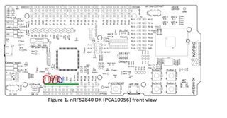
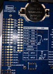
I have built the project and now I want to read some values from some voltages from one of the output pins in nRF52840 DK.

As suggested https://infocenter.nordicsemi.com/topic/com.nordic.infocenter.sdk5.v15.0.0/nrf_dev_saadc_example.html

(**To use VCC. In the hardware I see only VDD pins. Is it the same?)  in  

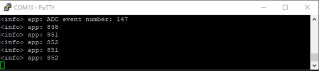
I tried to connect A0 pin to VDD (There are three VDD) pins however, value I read is,

<info> app: SAADC HAL simple example started.
<info> app: ADC event number: 0
<info> app: 19
<info> app: 19
<info> app: 18
<info> app: 19
<info> app: 17

However, if I connect to the 5V pin, I read,


<info> app: ADC event number: 22
<info> app: 559
<info> app: 560
<info> app: 559
<info> app: 560
<info> app: 559

Is it possible to know, why there is no output from the VDD pins? What is the expected voltage output of this pin?

Should I configure anything in the hardware?

Also is it ok to connect the 5V pin to the A0 pin?

Thanks a lot!!

Parents
  • There is only one VDD pin, on aQFN73 ball assignments it's A22, on WLCSP ball assignments it's B3. You're confusing regulator decoupling pins with a supply pin. 

    Also, Jörg is correct, you've likely fried the analog input when you supplied 5V to it, I suggest you consider it broken (for now) and use one of the other analog input pins when testing the SAADC. 

  • Hi Haakonsh/ Jorg,

    Thanks for the reply. Hope A0 pin is not burnt even though I connected to the 5V for few seconds. I first connected A0 pin to the 3.0 V. It still did not show a valid output.

    I was referring to the VDD pins in nRF52840 DK highlighted in Red in the above diagram. When I measured using the Multimeter it reads 3.0V. But ADC reading values don't seems to be correct. I simply connected a wire as shown above in Green.

    I am now using A1 pin. Still the same observation. Any idea what could be the reason? 

    Thanks a lot!!

  • Hi Haakonsh,

    Herewith attaching my source code and the hex file. It's the exact example from Nordic.

    saadc_nrf.rar

    Thank a lot!!

  • I measure ~850 when connected to VDD (~3.0V):

    With a gain of 1/6 and an internal voltage reference of 0.6V the input voltage range is 0-3.6V, and the expected output from an 3.0V input with 10-bit resolution is 3.0/3.6 * 1024 = 853.34. 

    If you do not see ~850 as the output when connecting the analog input to a 3V source then the pin is most likely fried. 

  • Hi,

    I now can see ~850 when I define NRF_SAADC_INPUT_AIN1 in the code and use pin "P0.03" to measure VDD (3.0V).

    However, when I define NRF_SAADC_INPUT_AIN0 I am unable to measure from pin "P0.03".

    Isn't "A0" = P0.03 = NRF_SAADC_INPUT_AIN0 ?

    If I define NRF_SAADC_INPUT_AIN2 in the code, I can use pin "P0.04" to measure VDD.


  • See Mapping of analog pins.

    AIN0 is the p0.02 pin on the opposite side of the DK. 

  • Hi, 

    Thanks for the reply. I have few more questions to clarify.

    1. The confusion happened because in my board it is printed as P0.03 (A0). Please see the attached images. So I thought NRF_SAADC_INPUT_AIN0 is for P0.03. In the other side of the board I see P0.02 (AREF). Is this the Pin for the channel NRF_SAADC_INPUT_AIN0? However AIN0 is not mentioned in the pin mapping table.

    2. If I define NRF_SAADC_INPUT_AIN0 as the channel, does it mean the ADC samples only from P0.02? Because initially I used P0.03 with the 5V, the reading was a low value than ~850. Maybe since it wasn't sampling from P0.03, it did not cause any damage. With AIN1 defined I still get a valid reading from P0.03 now.

    3. I observed that when I used NRF_SAADC_INPUT_AIN2 with P0.04, I get a larger fluctuation in the reading when nothing is connected to the pin P0.04. 

    <info> app: ADC event number: 141
    <info> app: -14
    <info> app: -6
    <info> app: -2
    <info> app: -18
    <info> app: -19
    <info> app: ADC event number: 142
    <info> app: 51
    <info> app: 289
    <info> app: 517
    <info> app: 736
    <info> app: 859

    However, if I connect to VDD or GND it measures the correct values. Is this normal?

    Thanks a lot!!

Reply
  • Hi, 

    Thanks for the reply. I have few more questions to clarify.

    1. The confusion happened because in my board it is printed as P0.03 (A0). Please see the attached images. So I thought NRF_SAADC_INPUT_AIN0 is for P0.03. In the other side of the board I see P0.02 (AREF). Is this the Pin for the channel NRF_SAADC_INPUT_AIN0? However AIN0 is not mentioned in the pin mapping table.

    2. If I define NRF_SAADC_INPUT_AIN0 as the channel, does it mean the ADC samples only from P0.02? Because initially I used P0.03 with the 5V, the reading was a low value than ~850. Maybe since it wasn't sampling from P0.03, it did not cause any damage. With AIN1 defined I still get a valid reading from P0.03 now.

    3. I observed that when I used NRF_SAADC_INPUT_AIN2 with P0.04, I get a larger fluctuation in the reading when nothing is connected to the pin P0.04. 

    <info> app: ADC event number: 141
    <info> app: -14
    <info> app: -6
    <info> app: -2
    <info> app: -18
    <info> app: -19
    <info> app: ADC event number: 142
    <info> app: 51
    <info> app: 289
    <info> app: 517
    <info> app: 736
    <info> app: 859

    However, if I connect to VDD or GND it measures the correct values. Is this normal?

    Thanks a lot!!

Children
Related