This post is older than 2 years and might not be relevant anymore
More Info: Consider searching for newer posts

nRF52840 DCCH/VDDH Pins for DCDC

Hi All,

I am trying to design a BLE module based on the nRF52840 Configuration 6 (Only Battery) provided in the product specification document.

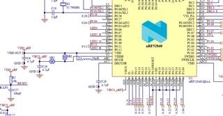
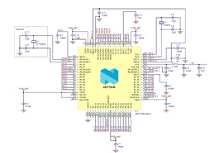
To get started I was using the footprint schematic provided by Nordic for the nRF52840 Dongle. It seems like pin positions of VDD and VDDH/ DCCH in the product specification document are different than in the Schematic provided for the Dongle. 

When I check the parts, the one provided in the Dongle schematic is "nRF52840-QIAAC0" and the one provided in the documentation is QIAA aQFNTm73. Please see the attached images below and few of my questions.


1. Which schematic/ footprint should I proceed with?

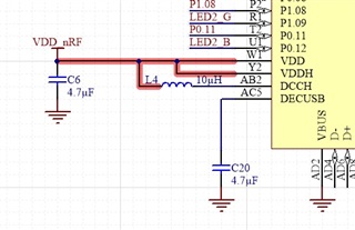
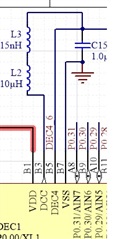
2. I am also planing to enable DCDC regulator if required. Is it ok to connect pins DCCH and VDD with a 10nH inductor, and DCC-DEC4 with series 15nH and 10uH inductors even if I don't use DCDC regulator? Please see the attachments below.


3. If I enable DCDC regulator, does it degrades RF performance? Will I have to use external RF amplification?

Thanks a lot!!

Parents
  • Hi,


    The nRF52840 power supply is flexible and can support multiple multiple configurations. This is perhaps best described in the PS: https://infocenter.nordicsemi.com/topic/ps_nrf52840/power.html?cp=4_0_0_4_2


    1) Depends on which kind of configuration you want to use the SoC in, and your supply rail. See the link above.

    2) When you short VDD and VDDH, you will disable the REG0 stage and thus the DCDC converter with output on DCCH. This config will work, but you will not be able to make use of the REG0 DCDC converter (DCCH), and can thus remove L4. If you want to use this you need to input on the VDDH pin only, not shorted with VDD. Like in ref.layout config 4: https://infocenter.nordicsemi.com/topic/ps_nrf52840/ref_circuitry.html?cp=4_0_0_6_2_3#unique_1073517861

    3) No, RF performance will not be affected if you use the onboard DCDC converters.


    Best regards,

    Andreas

  • Hi Andreas,

    Many thanks for the reply.

    1. I think my questions was not clear enough. Sorry about that. Actually the issue is the schematic diagram PIN positions. I am just not sure whether the layout pin positions also changes. As you can see in the first two images I have sent, VDDH, DCCH and VDD pin positions are different in two diagram. Is this just a schematic diagram or is there is a different chip variant I have to use in particularly?

    2. I checked the configuration 4. I am bit confused on the supply voltages. In this case:

       a) Actual supply voltage from the battery, should it be connected to VDD_HV or VDD_nRF?

       b) Does VDD pin acts as an output Voltage once I connect battery to VDD_HV?

Reply
  • Hi Andreas,

    Many thanks for the reply.

    1. I think my questions was not clear enough. Sorry about that. Actually the issue is the schematic diagram PIN positions. I am just not sure whether the layout pin positions also changes. As you can see in the first two images I have sent, VDDH, DCCH and VDD pin positions are different in two diagram. Is this just a schematic diagram or is there is a different chip variant I have to use in particularly?

    2. I checked the configuration 4. I am bit confused on the supply voltages. In this case:

       a) Actual supply voltage from the battery, should it be connected to VDD_HV or VDD_nRF?

       b) Does VDD pin acts as an output Voltage once I connect battery to VDD_HV?

Children
Related