
I can see in Segger Embedded Studio v4.52 under the Build Tab, there are two methods to build the project.
1- Build > Build zephyr/zephyr.elf
2- Build > Build solution
What is the difference between the two methods?
Kind regards
I can see in Segger Embedded Studio v4.52 under the Build Tab, there are two methods to build the project.
1- Build > Build zephyr/zephyr.elf
2- Build > Build solution
What is the difference between the two methods?
Kind regards
Hi again!
So, first of all, to answer your questions about SPI:
You are right, I did not catch that part. I have sent a message to the Nordic developer that has written this, but since they are based in LA I won't have an answer on this until tomorrow.
I just received an answer about this.
"An index representing the peripheral’s chip select line number. (If there is no chip select line, 0 is used.)"
The spi1 node has a cs-gpios property, which means that the unit addresses for node a and b (0 and 1 respectively) are indexes into the cs-gpios array (an index representing the peripheral's chip select line number). The spi1 node has no cs-gpios, so node c has no chip select configured in the device tree, and therefore its unit address is left at 0 (if there is no chip select line, 0 is used).
In all your overlay examples you're still instantiating the ADC peripheral, which we don't want to do.
This is the template you want to follow:
/ {
    n: node {
        compatible = " ";
        io-channels = <&adc 4>;
	    label = "AIN_0";
	};
};
The forward slash indicates the root node and is very important to include.
To include multiple ADC io-channels, just refer to the adc-node each time like this (not &adc5 and &adc7):
io-channels = <&adc 26>, <&adc 28>;
and if you want to use a different compatible property for the two nodes, you need to create two separate nodes like this:
/ {
    n: node_a {
        compatible = " ";
        io-channels = <&adc 26>;
	    label = "AIN_5";
	};

    n: node_b {
        compatible = " ";
        io-channels = <&adc 28>;
	    label = "AIN_7";
	};
};
For you question about voltage-divider
The lower leg is not a resistor, but the other one is a resistor? Or are you using a capacitive divider where both elements are capacitors?
For your binding question, yes this is the correct way to do it, using the label you defined in the node.
adc_dev_5 = device_get_binding("AIN_5");
adc_dev_7 = device_get_binding("AIN_7");
To do the binding for the two analog inputs, this is how to do it for AIN_5 and AIN_7 respectively.
device_get_binding(DT_IO_CHANNELS_LABEL_BY_IDX(DT_NODELABEL(n),0))
device_get_binding(DT_IO_CHANNELS_LABEL_BY_IDX(DT_NODELABEL(n),1))
Best regards,
Heidi
If I include in main.c
#include <hal/nrf_saadc.h>
and use this overlay file
&pwm0 {
ch0-pin = < 29 >;
};
/ {
n: node {
compatible = "voltage-divider";
io-channels = <&adc 4>;
label = "AIN_0";
};
};
then I get a different error,
devicetree error: 'output-ohms' is marked as required in 'properties:' in C:/Zypher/v1.3.0/zephyr/dts/bindings\adc\voltage-divider.yaml, but does not appear in <Node /node in 'nrf5340pdk_nrf5340_cpuapp.dts.pre.tmp'>
This suggests I need to add these two lines to the device tree fragment in the overlay file
output-ohms = <???>;
full-ohms = <(??? + ???)>;
But I am not sure if the "voltage-divider" works with an R-C circuit?
Finally, get_binding() does not bind AIN_0, it can only bind ADC_0.
Are you sure the label line can have something other than ADC_0?
Maybe I Should make changes to the source code (the light intensity controller example) in main.c when I am using the overlay file ?
Kind regards
Mohamed
So, this means channel_id = 0 i.e. index zero into the channel array points to AIN0.
Since it seems we have the channel_id index offset by one in the nRF5340PDK, does it mean the examples referred to will not work as expected?
According to the PCA10095_schematics of the nRF5340PDK pin P0.28 is AIN7. So, I connected a potentiometer to pins: P0.28, VDD, GND and tried to run the light intensity controller example but the adc did not work with this configuration code.
#define ADC_1ST_CHANNEL_ID 7
#define ADC_1ST_CHANNEL_INPUT NRF_SAADC_INPUT_AIN7
So, I looked closely to pin P0.28 on the back of the pdk board and realised that P0.28 is actually labelled (A2). So, I changed the config to,
#define ADC_1ST_CHANNEL_ID 2
#define ADC_1ST_CHANNEL_INPUT NRF_SAADC_INPUT_AIN2
and Bingo! it works. So, it seems that for the nRF5340PDK the values used for ADC_1ST_CHANNEL_ID and ADC_1ST_CHANNEL_INPUT must the same. Any comments?
Kind regards
Mohamed
Hi!
You know what, I misunderstood the description of channel_id. Sorry about that.
At a closer look: "This value primarily identifies the channel within the ADC API". So the value of the channel_id does not matter (in the range of 0 to 7) as long as it is used consistently to identify that channel. This explains why channel ID 0 is used for AIN0 and channel 2 is used for AIN2, here.
My mistake, sorry for the confusion! There is no channel id offset and the sample should work as expected.
Yes, the table I linked to is apparently incorrect, so this is the correct pin mapping.
| AIN0 | P0.04 |
| AIN1 | P0.05 |
| AIN2 | P0.06 |
| AIN3 | P0.07 |
| AIN4 | P0.25 |
| AIN5 | P0.26 |
| AIN6 | P0.27 |
| AIN7 | P0.28 |
Learner said:Bingo! it works.
Did it work with the analog device plugged into GPIO pin 28 or pin 6?
If it was pin 28, could you attach the file with the path build_folder/zephyr/zephyr.dts just so I can confirm this?
Again, sorry for the confusion.
Best regards,
Heidi
Hi Heidi,
No problem, we are all learning in the process.
At a closer look: "This value primarily identifies the channel within the ADC API". So the value of the channel_id does not matter (in the range of 0 to 7) as long as it is used consistently to identify that channel. This explains why channel ID 0 is used for AIN0 and channel 2 is used for AIN2, here.
I am not sure I understand what you are trying to say here.
I understand the need to configure which analog pin is being used but I am still not clear on which one of these two macros is doing this job. If as you said it is ADC_1ST_CHANNEL_INPUT then why is ADC_1ST_CHANNEL_ID needed?
The best way to understand what channel_id does is to see where it is used in the driver code. There is a driver function called channel_setup but I could not locate it. Could you please ask your colleagues developers to point us where in the driver code this function that uses channel_id and channel_input is.
Thank you.
Kind regards
Mohamed
Did it work with the analog device plugged into GPIO pin 28 or pin 6?
It was pin P0.28. I could not insert the dts file as attachment, so, I am pasting its content instead.
/dts-v1/;

/ {
#address-cells = < 0x1 >;
#size-cells = < 0x1 >;
model = "Nordic NRF5340 PDK NRF5340 Application";
compatible = "nordic,nrf5340-pdk-nrf5340-cpuapp", "nordic,nrf5340-cpuapp-qkaa", "nordic,nrf5340-cpuapp";
chosen {
zephyr,flash-controller = &flash_controller;
zephyr,console = &uart0;
zephyr,shell-uart = &uart0;
zephyr,uart-mcumgr = &uart0;
zephyr,bt-mon-uart = &uart0;
zephyr,bt-c2h-uart = &uart0;
zephyr,ipc_shm = &sram0_shared;
zephyr,sram = &sram0_image;
zephyr,flash = &flash0;
zephyr,code-partition = &slot0_partition;
zephyr,sram-secure-partition = &sram0_s;
zephyr,sram-non-secure-partition = &sram0_ns;
};
aliases {
flash-controller = &flash_controller;
rtc-0 = &rtc0;
rtc-1 = &rtc1;
uart-0 = &uart0;
uart-1 = &uart1;
uart-2 = &uart2;
uart-3 = &uart3;
adc-0 = &adc;
egu-0 = &egu0;
egu-1 = &egu1;
egu-2 = &egu2;
egu-3 = &egu3;
egu-4 = &egu4;
egu-5 = &egu5;
gpio-0 = &gpio0;
gpio-1 = &gpio1;
gpiote-0 = &gpiote;
i2c-0 = &i2c0;
i2c-1 = &i2c1;
i2c-2 = &i2c2;
i2c-3 = &i2c3;
ipc-0 = &ipc;
pdm-0 = &pdm0;
spi-0 = &spi0;
spi-1 = &spi1;
spi-2 = &spi2;
spi-3 = &spi3;
spi-4 = &spi4;
pwm-0 = &pwm0;
pwm-1 = &pwm1;
pwm-2 = &pwm2;
pwm-3 = &pwm3;
wdt-0 = &wdt;
timer-0 = &timer0;
timer-1 = &timer1;
timer-2 = &timer2;
led0 = &led0;
led1 = &led1;
led2 = &led2;
led3 = &led3;
sw0 = &button0;
sw1 = &button1;
sw2 = &button2;
sw3 = &button3;
};
soc {
#address-cells = < 0x1 >;
#size-cells = < 0x1 >;
compatible = "nordic,nRF5340-CPU0-QKAA", "nordic,nRF5340-CPU0", "nordic,nRF53", "simple-bus";
interrupt-parent = < &nvic >;
ranges;
nvic: interrupt-controller@e000e100 {
compatible = "arm,v8m-nvic";
reg = < 0xe000e100 0xc00 >;
interrupt-controller;
#interrupt-cells = < 0x2 >;
arm,num-irq-priority-bits = < 0x3 >;
phandle = < 0x1 >;
};
systick: timer@e000e010 {
compatible = "arm,armv8m-systick";
reg = < 0xe000e010 0x10 >;
status = "disabled";
};
sram0: memory@20000000 {
device_type = "memory";
compatible = "mmio-sram";
reg = < 0x20000000 0x80000 >;
};
peripheral@50000000 {
#address-cells = < 0x1 >;
#size-cells = < 0x1 >;
ranges = < 0x0 0x50000000 0x10000000 >;
flash_controller: flash-controller@39000 {
compatible = "nordic,nrf53-flash-controller";
reg = < 0x39000 0x1000 >;
#address-cells = < 0x1 >;
#size-cells = < 0x1 >;
label = "NRF_FLASH_DRV_NAME";
flash0: flash@0 {
compatible = "soc-nv-flash";
label = "NRF_FLASH";
erase-block-size = < 0x1000 >;
write-block-size = < 0x4 >;
reg = < 0x0 0x100000 >;
partitions {
compatible = "fixed-partitions";
#address-cells = < 0x1 >;
#size-cells = < 0x1 >;
boot_partition: partition@0 {
label = "mcuboot";
reg = < 0x0 0x10000 >;
};
slot0_partition: partition@10000 {
label = "image-0";
reg = < 0x10000 0x30000 >;
};
slot0_ns_partition: partition@40000 {
label = "image-0-nonsecure";
reg = < 0x40000 0x40000 >;
};
slot1_partition: partition@80000 {
label = "image-1";
reg = < 0x80000 0x30000 >;
};
slot1_ns_partition: partition@b0000 {
label = "image-1-nonsecure";
reg = < 0xb0000 0x40000 >;
};
scratch_partition: partition@f0000 {
label = "image-scratch";
reg = < 0xf0000 0xa000 >;
};
storage_partition: partition@fa000 {
label = "storage";
reg = < 0xfa000 0x6000 >;
};
};
};
};
adc: adc@e000 {
compatible = "nordic,nrf-saadc";
reg = < 0xe000 0x1000 >;
interrupts = < 0xe 0x1 >;
status = "okay";
label = "ADC_0";
#io-channel-cells = < 0x1 >;
};
dppic: dppic@17000 {
compatible = "nordic,nrf-dppic";
reg = < 0x17000 0x1000 >;
status = "okay";
label = "DPPIC";
};
egu0: egu@1b000 {
compatible = "nordic,nrf-egu";
reg = < 0x1b000 0x1000 >;
interrupts = < 0x1b 0x1 >;
status = "okay";
};
egu1: egu@1c000 {
compatible = "nordic,nrf-egu";
reg = < 0x1c000 0x1000 >;
interrupts = < 0x1c 0x1 >;
status = "okay";
};
egu2: egu@1d000 {
compatible = "nordic,nrf-egu";
reg = < 0x1d000 0x1000 >;
interrupts = < 0x1d 0x1 >;
status = "okay";
};
egu3: egu@1e000 {
compatible = "nordic,nrf-egu";
reg = < 0x1e000 0x1000 >;
interrupts = < 0x1e 0x1 >;
status = "okay";
};
egu4: egu@1f000 {
compatible = "nordic,nrf-egu";
reg = < 0x1f000 0x1000 >;
interrupts = < 0x1f 0x1 >;
status = "okay";
};
egu5: egu@20000 {
compatible = "nordic,nrf-egu";
reg = < 0x20000 0x1000 >;
interrupts = < 0x20 0x1 >;
status = "okay";
};
i2s0: i2s@28000 {
compatible = "nordic,nrf-i2s";
#address-cells = < 0x1 >;
#size-cells = < 0x0 >;
reg = < 0x28000 0x1000 >;
interrupts = < 0x28 0x1 >;
status = "disabled";
label = "I2S_0";
};
ipc: ipc@2a000 {
compatible = "nordic,nrf-ipc";
reg = < 0x2a000 0x1000 >;
interrupts = < 0x2a 0x1 >;
status = "okay";
label = "IPC";
};
kmu: kmu@39000 {
compatible = "nordic,nrf-kmu";
reg = < 0x39000 0x1000 >;
interrupts = < 0x39 0x1 >;
status = "okay";
};
pdm0: pdm@26000 {
compatible = "nordic,nrf-pdm";
reg = < 0x26000 0x1000 >;
interrupts = < 0x26 0x1 >;
status = "disabled";
label = "PDM_0";
};
regulators: regulator@4000 {
compatible = "nordic,nrf-regulators";
reg = < 0x4000 0x1000 >;
status = "okay";
};
vmc: vmc@81000 {
compatible = "nordic,nrf-vmc";
reg = < 0x81000 0x1000 >;
status = "okay";
};
uart0: uart@8000 {
compatible = "nordic,nrf-uarte";
reg = < 0x8000 0x1000 >;
interrupts = < 0x8 0x1 >;
status = "okay";
label = "UART_0";
current-speed = < 0x1c200 >;
tx-pin = < 0x14 >;
rx-pin = < 0x16 >;
rts-pin = < 0x13 >;
cts-pin = < 0x15 >;
};
uart1: uart@9000 {
compatible = "nordic,nrf-uarte";
reg = < 0x9000 0x1000 >;
interrupts = < 0x9 0x1 >;
status = "disabled";
label = "UART_1";
};
uart2: uart@b000 {
compatible = "nordic,nrf-uarte";
reg = < 0xb000 0x1000 >;
interrupts = < 0xb 0x1 >;
status = "disabled";
label = "UART_2";
};
uart3: uart@c000 {
compatible = "nordic,nrf-uarte";
reg = < 0xc000 0x1000 >;
interrupts = < 0xc 0x1 >;
status = "disabled";
label = "UART_3";
};
i2c0: i2c@8000 {
#address-cells = < 0x1 >;
#size-cells = < 0x0 >;
reg = < 0x8000 0x1000 >;
clock-frequency = < 0x186a0 >;
interrupts = < 0x8 0x1 >;
status = "disabled";
label = "I2C_0";
};
i2c1: i2c@9000 {
#address-cells = < 0x1 >;
#size-cells = < 0x0 >;
reg = < 0x9000 0x1000 >;
clock-frequency = < 0x186a0 >;
interrupts = < 0x9 0x1 >;
status = "okay";
label = "I2C_1";
compatible = "nordic,nrf-twim";
sda-pin = < 0x1e >;
scl-pin = < 0x1f >;
};
i2c2: i2c@b000 {
#address-cells = < 0x1 >;
#size-cells = < 0x0 >;
reg = < 0xb000 0x1000 >;
clock-frequency = < 0x186a0 >;
interrupts = < 0xb 0x1 >;
status = "disabled";
label = "I2C_2";
};
i2c3: i2c@c000 {
#address-cells = < 0x1 >;
#size-cells = < 0x0 >;
reg = < 0xc000 0x1000 >;
clock-frequency = < 0x186a0 >;
interrupts = < 0xc 0x1 >;
status = "disabled";
label = "I2C_3";
};
spi0: spi@8000 {
#address-cells = < 0x1 >;
#size-cells = < 0x0 >;
reg = < 0x8000 0x1000 >;
interrupts = < 0x8 0x1 >;
status = "disabled";
label = "SPI_0";
};
spi1: spi@9000 {
#address-cells = < 0x1 >;
#size-cells = < 0x0 >;
reg = < 0x9000 0x1000 >;
interrupts = < 0x9 0x1 >;
status = "disabled";
label = "SPI_1";
};
spi2: spi@b000 {
#address-cells = < 0x1 >;
#size-cells = < 0x0 >;
reg = < 0xb000 0x1000 >;
interrupts = < 0xb 0x1 >;
status = "okay";
label = "SPI_2";
compatible = "nordic,nrf-spim";
sck-pin = < 0x20 >;
mosi-pin = < 0x20 >;
miso-pin = < 0x24 >;
};
spi3: spi@c000 {
#address-cells = < 0x1 >;
#size-cells = < 0x0 >;
reg = < 0xc000 0x1000 >;
interrupts = < 0xc 0x1 >;
status = "disabled";
label = "SPI_3";
};
spi4: spi@a000 {
compatible = "nordic,nrf-spim";
#address-cells = < 0x1 >;
#size-cells = < 0x0 >;
reg = < 0xa000 0x1000 >;
interrupts = < 0xa 0x1 >;
status = "disabled";
label = "SPI_4";
};
pwm0: pwm@21000 {
compatible = "nordic,nrf-pwm";
reg = < 0x21000 0x1000 >;
interrupts = < 0x21 0x1 >;
status = "okay";
label = "PWM_0";
#pwm-cells = < 0x1 >;
ch0-pin = < 0x1c >;
};
pwm1: pwm@22000 {
compatible = "nordic,nrf-pwm";
reg = < 0x22000 0x1000 >;
interrupts = < 0x22 0x1 >;
status = "disabled";
label = "PWM_1";
#pwm-cells = < 0x1 >;
};
pwm2: pwm@23000 {
compatible = "nordic,nrf-pwm";
reg = < 0x23000 0x1000 >;
interrupts = < 0x23 0x1 >;
status = "disabled";
label = "PWM_2";
#pwm-cells = < 0x1 >;
};
pwm3: pwm@24000 {
compatible = "nordic,nrf-pwm";
reg = < 0x24000 0x1000 >;
interrupts = < 0x24 0x1 >;
status = "disabled";
label = "PWM_3";
#pwm-cells = < 0x1 >;
};
gpio0: gpio@842500 {
compatible = "nordic,nrf-gpio";
gpio-controller;
reg = < 0x842500 0x300 >;
#gpio-cells = < 0x2 >;
label = "GPIO_0";
status = "okay";
phandle = < 0x2 >;
};
gpio1: gpio@842800 {
compatible = "nordic,nrf-gpio";
gpio-controller;
reg = < 0x842800 0x300 >;
#gpio-cells = < 0x2 >;
ngpios = < 0x10 >;
label = "GPIO_1";
status = "okay";
};
rtc0: rtc@14000 {
compatible = "nordic,nrf-rtc";
reg = < 0x14000 0x1000 >;
interrupts = < 0x14 0x1 >;
status = "okay";
clock-frequency = < 0x8000 >;
prescaler = < 0x1 >;
label = "RTC_0";
};
rtc1: rtc@15000 {
compatible = "nordic,nrf-rtc";
reg = < 0x15000 0x1000 >;
interrupts = < 0x15 0x1 >;
status = "okay";
clock-frequency = < 0x8000 >;
prescaler = < 0x1 >;
label = "RTC_1";
};
clock: clock@5000 {
compatible = "nordic,nrf-clock";
reg = < 0x5000 0x1000 >;
interrupts = < 0x5 0x1 >;
status = "okay";
label = "CLOCK";
};
power: power@5000 {
compatible = "nordic,nrf-power";
reg = < 0x5000 0x1000 >;
interrupts = < 0x5 0x1 >;
status = "okay";
};
wdt: wdt0: watchdog@18000 {
compatible = "nordic,nrf-watchdog";
reg = < 0x18000 0x1000 >;
interrupts = < 0x18 0x1 >;
status = "okay";
label = "WDT";
};
wdt1: watchdog@19000 {
compatible = "nordic,nrf-watchdog";
reg = < 0x19000 0x1000 >;
interrupts = < 0x19 0x1 >;
status = "disabled";
label = "WDT_1";
};
timer0: timer@f000 {
compatible = "nordic,nrf-timer";
status = "okay";
reg = < 0xf000 0x1000 >;
interrupts = < 0xf 0x1 >;
prescaler = < 0x0 >;
label = "TIMER_0";
};
timer1: timer@10000 {
compatible = "nordic,nrf-timer";
status = "okay";
reg = < 0x10000 0x1000 >;
interrupts = < 0x10 0x1 >;
prescaler = < 0x0 >;
label = "TIMER_1";
};
timer2: timer@11000 {
compatible = "nordic,nrf-timer";
status = "okay";
reg = < 0x11000 0x1000 >;
interrupts = < 0x11 0x1 >;
prescaler = < 0x0 >;
label = "TIMER_2";
};
};
cryptocell: crypto@50844000 {
compatible = "nordic,nrf-cc312";
reg = < 0x50844000 0x1000 >;
label = "CRYPTOCELL";
status = "okay";
#address-cells = < 0x1 >;
#size-cells = < 0x1 >;
cryptocell312: crypto@50845000 {
compatible = "arm,cryptocell-312";
reg = < 0x50845000 0x1000 >;
interrupts = < 0x44 0x1 >;
label = "CRYPTOCELL312";
};
};
gpiote: gpiote@5000d000 {
compatible = "nordic,nrf-gpiote";
reg = < 0x5000d000 0x1000 >;
interrupts = < 0xd 0x5 >;
status = "okay";
label = "GPIOTE_0";
};
spu: spu@50003000 {
compatible = "nordic,nrf-spu";
reg = < 0x50003000 0x1000 >;
interrupts = < 0x3 0x1 >;
status = "okay";
};
ficr: ficr@ff0000 {
compatible = "nordic,nrf-ficr";
reg = < 0xff0000 0x1000 >;
status = "okay";
};
uicr: uicr@ff8000 {
compatible = "nordic,nrf-uicr";
reg = < 0xff8000 0x1000 >;
status = "okay";
};
};
cpus {
#address-cells = < 0x1 >;
#size-cells = < 0x0 >;
cpu@0 {
device_type = "cpu";
compatible = "arm,cortex-m33f";
reg = < 0x0 >;
#address-cells = < 0x1 >;
#size-cells = < 0x1 >;
mpu: mpu@e000ed90 {
compatible = "arm,armv8m-mpu";
reg = < 0xe000ed90 0x40 >;
arm,num-mpu-regions = < 0x10 >;
};
};
};
leds {
compatible = "gpio-leds";
led0: led_0 {
gpios = < &gpio0 0x1c 0x1 >;
label = "Green LED 0";
};
led1: led_1 {
gpios = < &gpio0 0x1d 0x1 >;
label = "Green LED 1";
};
led2: led_2 {
gpios = < &gpio0 0x1e 0x1 >;
label = "Green LED 2";
};
led3: led_3 {
gpios = < &gpio0 0x1f 0x1 >;
label = "Green LED 3";
};
};
buttons {
compatible = "gpio-keys";
button0: button_0 {
gpios = < &gpio0 0x17 0x11 >;
label = "Push button 1";
};
button1: button_1 {
gpios = < &gpio0 0x18 0x11 >;
label = "Push button 2";
};
button2: button_2 {
gpios = < &gpio0 0x8 0x11 >;
label = "Push button 3";
};
button3: button_3 {
gpios = < &gpio0 0x9 0x11 >;
label = "Push button 4";
};
};
reserved-memory {
#address-cells = < 0x1 >;
#size-cells = < 0x1 >;
ranges;
sram0_image: image@20000000 {
reg = < 0x20000000 0x70000 >;
};
sram0_s: image_s@20000000 {
reg = < 0x20000000 0x10000 >;
};
sram0_ns: image_ns@20010000 {
reg = < 0x20010000 0x60000 >;
};
sram0_shared: memory@20070000 {
reg = < 0x20070000 0x10000 >;
};
};
};Hi!
So according to the analog inputs and channels page for the nRF5340, there are eight analog input channels that can be configured CH[n] (n=0, 1, .., 7).
There are also eight analog inputs available (AIN0, AIN1, ... AIN7) and VDD and VDDHDIV5.
So the channel_id refers to one of the eight analog input channels and the channel_input refers to an analog input. That is the difference.
There are 8 identical analog input channels and you can use whichever one you want and you can configure that channel with any analog input you want. They are not "connected" as I initially thought, where channel 0 uses AIN0 and so forth.
If it helps you understand better, here is how the channel_id is used in the code.
So the function adc_nrfx_channel_setup(const struct device *dev, const struct adc_channel_cfg *channel_cfg)
is called, where channel_id is one of the properties in the adc_channel_cfg struct.
Then, in this function, the channel_id is passed to nrf_saadc_channel_init(), here. If you take a look at the function definition, you can see the channel ID is being used the select the correct CH[n].CONFIG register to add all the configurations.
p_reg->CH[channel].CONFIG =
The positive input isn't set until the start_read() function is called. Then the function nrf_saadc_channel_pos_input_set() is called here. If we take a look at this function definition:
p_reg->CH[channel].PSELP = pselp;

where
NRF_SAADC_Type * p_reg = NRF_SAADC
uint8_t channel = ADC_1ST_CHANNEL_ID
nrf_saadc_input_t pselp = ADC_1ST_CHANNEL_INPUT
we can see that it uses the channel ID to the specific channel to be associated with the analog input passed to the function (ADC_1ST_CHANNEL_ID).
So for instance you can set NRFSAADC->CH[0].PSELP = NRF_SAADC_INPUT_AIN7 without a problem.
Learner said:If as you said it is ADC_1ST_CHANNEL_INPUT then why is ADC_1ST_CHANNEL_ID needed?
So to answer this question it's because the channel ID specifies which of the analog input channels you are referring to and is used with the register CH[channel_id].PSELP and CH[channel_id].CONFIG. And the channel input defines which analog input to "attach" to that channel.
So CH[CHANNEL_ID].PSELP = CHANNEL_INPUT.
Learner said:So, it seems that for the nRF5340PDK the values used for ADC_1ST_CHANNEL_ID and ADC_1ST_CHANNEL_INPUT must the same. Any
No, they do not need to be the same. You do however need to be connected to the correct GPIO pin.
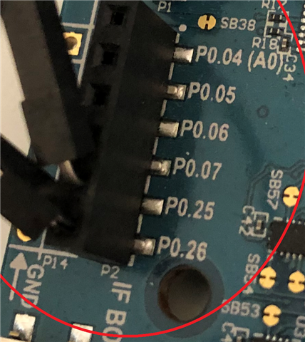
Learner said:So, I looked closely to pin P0.28 on the back of the pdk board and realised that P0.28 is actually labelled (A2)
Those labels are just the arduino naming and don't correspond to the analog inputs.
It also looks like the printing on back of the board and the front of the board don't match up.
The front of the board has the correct labeling, so if you are plugged into the pin with the P0.08 label on the back, you are actually connected to P0.06 which is AIN2. So at least that mystery is solved!
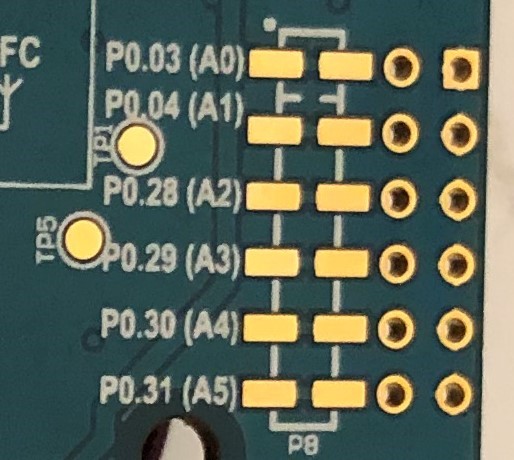
Also, on the nRF5340 PDK GPIO P0.28 (AIN7) is also used for LED1. To be able to use AIN7, you will need to cut SB5 on the board, see here.
Best regards,
Heidi
Hi!
So according to the analog inputs and channels page for the nRF5340, there are eight analog input channels that can be configured CH[n] (n=0, 1, .., 7).
There are also eight analog inputs available (AIN0, AIN1, ... AIN7) and VDD and VDDHDIV5.
So the channel_id refers to one of the eight analog input channels and the channel_input refers to an analog input. That is the difference.
There are 8 identical analog input channels and you can use whichever one you want and you can configure that channel with any analog input you want. They are not "connected" as I initially thought, where channel 0 uses AIN0 and so forth.
If it helps you understand better, here is how the channel_id is used in the code.
So the function adc_nrfx_channel_setup(const struct device *dev, const struct adc_channel_cfg *channel_cfg)
is called, where channel_id is one of the properties in the adc_channel_cfg struct.
Then, in this function, the channel_id is passed to nrf_saadc_channel_init(), here. If you take a look at the function definition, you can see the channel ID is being used the select the correct CH[n].CONFIG register to add all the configurations.
p_reg->CH[channel].CONFIG =
The positive input isn't set until the start_read() function is called. Then the function nrf_saadc_channel_pos_input_set() is called here. If we take a look at this function definition:
p_reg->CH[channel].PSELP = pselp;

where
NRF_SAADC_Type * p_reg = NRF_SAADC
uint8_t channel = ADC_1ST_CHANNEL_ID
nrf_saadc_input_t pselp = ADC_1ST_CHANNEL_INPUT
we can see that it uses the channel ID to the specific channel to be associated with the analog input passed to the function (ADC_1ST_CHANNEL_ID).
So for instance you can set NRFSAADC->CH[0].PSELP = NRF_SAADC_INPUT_AIN7 without a problem.
Learner said:If as you said it is ADC_1ST_CHANNEL_INPUT then why is ADC_1ST_CHANNEL_ID needed?
So to answer this question it's because the channel ID specifies which of the analog input channels you are referring to and is used with the register CH[channel_id].PSELP and CH[channel_id].CONFIG. And the channel input defines which analog input to "attach" to that channel.
So CH[CHANNEL_ID].PSELP = CHANNEL_INPUT.
Learner said:So, it seems that for the nRF5340PDK the values used for ADC_1ST_CHANNEL_ID and ADC_1ST_CHANNEL_INPUT must the same. Any
No, they do not need to be the same. You do however need to be connected to the correct GPIO pin.
Learner said:So, I looked closely to pin P0.28 on the back of the pdk board and realised that P0.28 is actually labelled (A2)
Those labels are just the arduino naming and don't correspond to the analog inputs.
It also looks like the printing on back of the board and the front of the board don't match up.
The front of the board has the correct labeling, so if you are plugged into the pin with the P0.08 label on the back, you are actually connected to P0.06 which is AIN2. So at least that mystery is solved!
Also, on the nRF5340 PDK GPIO P0.28 (AIN7) is also used for LED1. To be able to use AIN7, you will need to cut SB5 on the board, see here.
Best regards,
Heidi
Hi Heidi,
Thank you. It is much clearer now.
p_reg->CH[channel].PSELP = pselp;
where
NRF_SAADC_Type * p_reg = NRF_SAADC
uint8_t channel = ADC_1ST_CHANNEL_ID
nrf_saadc_input_t pselp = ADC_1ST_CHANNEL_ID
I think you meant to say nrf_saadc_input_t pselp = ADC_1ST_CHANNEL_INPUT. Right?
Kind regards
Mohamed
Yes absolutely! I have changed it now. :)
Thank you Heidi.
I would like to 'Verify Answer' but there bits bits of information spread over multiple posts. One way to do this would be to add the bits of missing information to the post that has most of the correct info. Please let me know and I will Verify.
Kind regards
Mohamed

