
I’m obviously missing something from the information I’ve gathered with respect to designing a co-planar waveguide, PCB 50 Ohm transmission line. The calculations I get differ greatly from that of what I measure reviewing Nordic provided Gerber files. Links Provided Below
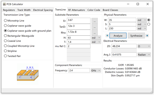
Using AppCAD and KiCad calculator (both yield the same results) I do get the same width and spacing value as that measured in the Nordic Gerber files – IF the calculations were made using a board thickness of 63mil. However, the 4 layer PCB indicates that both the inner copper and bottom copper are solid ground planes under the transmission line. This would suggest that the actual PCB layer over a ground plane from the transmission line is 6.7 mil not the full thickness of the board (63mil.)
As the mitigating component is the dialectic of the PCB material (190Tg FR408-HR – 3.67) and the inner-layer PCB has a thickness of 6.7 mil the numbers would be different. Changing the height measurement and substrate dialectic solves the problem – sort of – at least the numbers are much closer to what I expect.
Taking into the consideration that there are several ground planes below the transmission line my question is how are the Nordic files calculated?
I’m assuming I can use my values from this post: https://devzone.nordicsemi.com/f/nordic-q-a/10689/50-ohm-track-for-4-pcb-layer-nrf51822-qfac
Here are my calculations:
Note that changing the dialectic between 4.5 and 3.67 changes the impedance by around 5 Ohms.
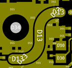
nRF52840 Dongle - HW files 1_0_0.zip (measuring around D13)
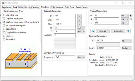
Using a board thickness of 6.7 mils
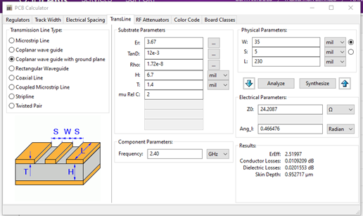
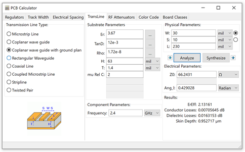
Using a board thickness of 63 mil:
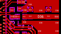
nRF52840-QIAA Reference Layout 1_1.zip
(looking in the Production files directory - nrf52840_qiaa_var2.GTL file – measuring around D36)
Using a board thickness of 6.7 mils
Using a board thickness of 63 mil:
Links:
https://devzone.nordicsemi.com/f/nordic-q-a/10689/50-ohm-track-for-4-pcb-layer-nrf51822-qfac
https://www.disk91.com/2015/technology/hardware/design-a-50ohm-impedance-net-for-rf-signals/
https://docs.oshpark.com/services/four-layer/
So - What am I missing? Can I be reading the Gerber files incorrectly?
