This post is older than 2 years and might not be relevant anymore
More Info: Consider searching for newer posts

nRF52840 Design Review Request

Hi,

We are developing nRF52840 based design with PCB antenna.

Please review the Schematic and PCB file.

Regards,

IrfanMeshtek_nRF52840_V1.0 PCB ANT_SCH.pdf20210607_nRF52840 Layout.PcbDoc
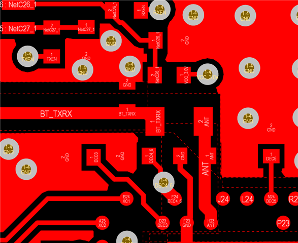
Parents
  • Hi Irfan

    I've taken a look at the design. The schematic is ok, no issues that I can see. For the layout, I have a few comments: 

    1 You should remove he cut outs on the inner layers. You need to have some shielding under the RF section and the inner ground layer can do that. 

    2. Move C13 closer to the ANT pin as the track is too long. Also move L2 and C2 closer to reduce the track length between the components. Something like this: 

    Else it looks good.

    best regards,

    Ketil Aas-Johansen

Reply
  • Hi Irfan

    I've taken a look at the design. The schematic is ok, no issues that I can see. For the layout, I have a few comments: 

    1 You should remove he cut outs on the inner layers. You need to have some shielding under the RF section and the inner ground layer can do that. 

    2. Move C13 closer to the ANT pin as the track is too long. Also move L2 and C2 closer to reduce the track length between the components. Something like this: 

    Else it looks good.

    best regards,

    Ketil Aas-Johansen

Children
No Data
Related