This post is older than 2 years and might not be relevant anymore
More Info: Consider searching for newer posts

Designing my PCB with nRF51822 and onchip antenna/ Performance

Hi,

I'm gonna make my first attemp with the RF 2.4GHZ antenna, and want to get a good performace for the RF transmission meaning minimum loss of the power transmission and the maximum range as possible. I'm using the NRF51822-QFAA-R7 Bluetooth Smart with the Johanson Technology Balun the 2450BM14E0003T and the 2450AT43A100E as the antenna :

www.johansontechnology.com/.../2450BM14E0003.pdf

www.johansontechnology.com/.../2450AT43A100.pdf

The first thing i start by calculating the Line width to match the 50Ω characteristic impedance. its mandatory to know the PCB material, for that i'm gonna use the 2 PCB layer from OSHPARK. their characteristic for PCB are :

  • All 2 boards are FR4 170Tg/290Td

  • They’re 1.6mm thick (0.063 inches) with 1 ounce copper on both sides.

using the AppCad software i tried to calculate the trace width , the result are bellow :

image description

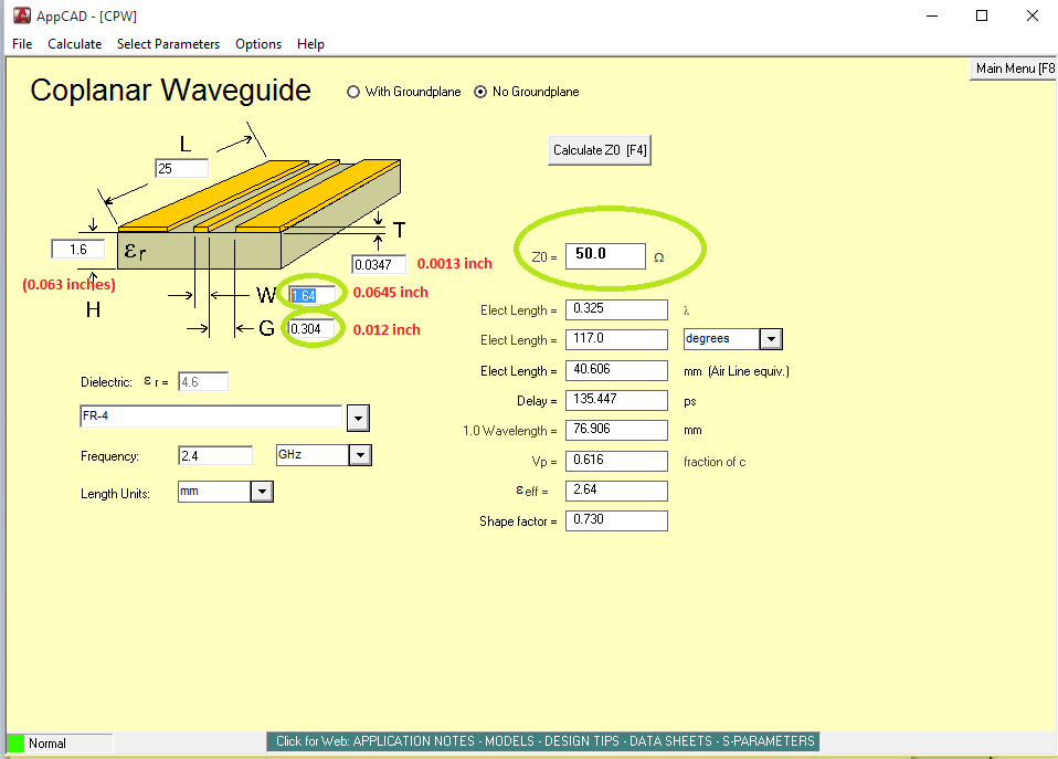
the size are they correct ?

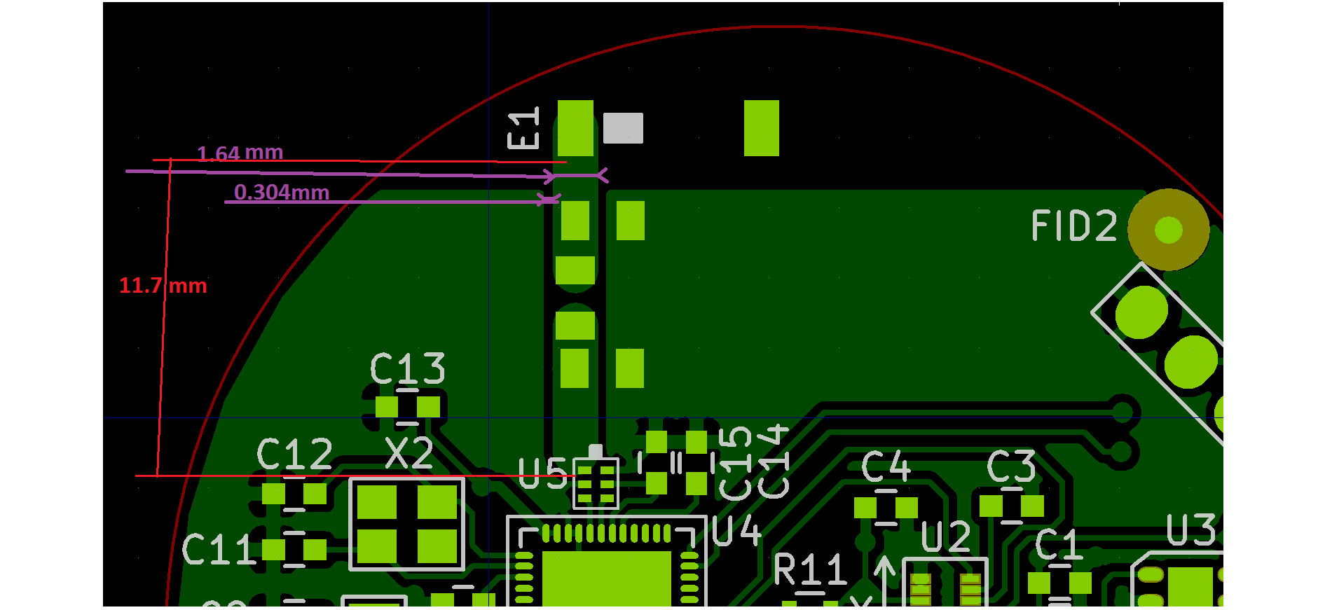
and this is how its looks like my PCB

image description

i put also a PI network and i didn't know how can i guess approximately the value of the PI netwrok ?? or should i put a shunt resistor with 0 Ohm then use the Spectrum analyzer ? is there other solution than using Spectrum analyzer to tune the antenna ??

What do you think about the PCB ? can i have a chance to get a good RF transmission ?

Parents
  • Hi Tizana,

    Why don't you have ground on the bottom layer ? Having proper ground improves RF performance.

    Other than that your schematic and layout look good.

    To be able to find the value for the PI network (to tune the antenna to meet 50 Ohm impedance because the environment, such as plastic case, housing will affect the antenna), you would need the network analyzer. The spectrum analyzer would not be sufficient.

    However, you can send your prototype to us. We will to the turning for you and send you the value of the tuning network (and the prototype )back.

    If you just want to have a prototype that works with OK range, your design should be fine. Just use 0Ohm resistor for the series component in the PI network and leave the other 2 open.

  • You can open a case in our support portal (Click My Page on our website). In the case you can request a final review when we are OK with the design, you can make the prototype and send it to us with the address and attention provided in the case.

  • Dear Hung


    Can you please review the attached schematic of NRF51822 used with matching Balun and chip antenna.


    Balun: 2450BM14E0003T

    Chip Antenna: 2450AT18A100E (T matching network)


    Please help to solve below queries:

    1. Please confirm chip antenna used with a balun, will that work? Suggest matching chip antenna if I am wrong.

    2. Is it ok to use R6 ( 0R ) in series with balun?

    3. Pin 31 (ANT1) and Pin 32 (ANT2) are to be routed differential?

    4. Please share design guidelines for Balun and Chip Antenna for good RF performance.

    5. Please share the reference design for the same.

    nrf51822.pdf

Reply
  • Dear Hung


    Can you please review the attached schematic of NRF51822 used with matching Balun and chip antenna.


    Balun: 2450BM14E0003T

    Chip Antenna: 2450AT18A100E (T matching network)


    Please help to solve below queries:

    1. Please confirm chip antenna used with a balun, will that work? Suggest matching chip antenna if I am wrong.

    2. Is it ok to use R6 ( 0R ) in series with balun?

    3. Pin 31 (ANT1) and Pin 32 (ANT2) are to be routed differential?

    4. Please share design guidelines for Balun and Chip Antenna for good RF performance.

    5. Please share the reference design for the same.

    nrf51822.pdf

Children
Related