4 second current spikes during sleep

Hello All,

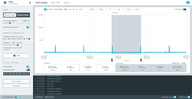
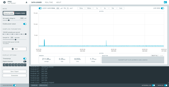
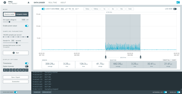
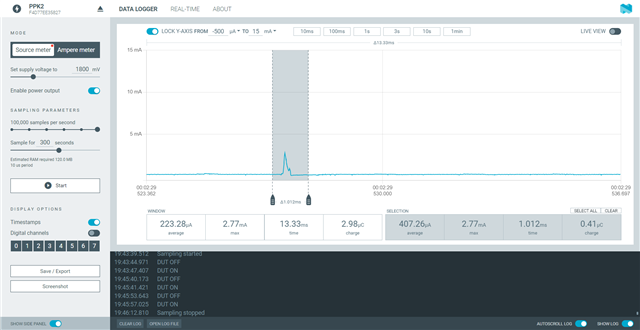
I am getting these ~3.5mA current spikes very 4 seconds and I can't seem to figure what the cause of them is. some of the spikes have a single spike/pulse while other have multiple. please see the attached images. I have commented out everything except the while in the main function and no difference. I have also commented out the enabling of the DCDC and still the same issue. any help would be greatly appreciate. I have a feeling its in the project config setting but tried commenting out what I thought may be the cause but no change either. 

I am using a custom board with 52833 and nRF Connect SDK 2.0.0. the board does have other ICs(hall sensors) but I measured their consumption and had no spikes.

while (1) {
		//k_sleep(K_SECONDS(1));
		//k_msleep(500);
		
		__WFE();
}

my project config file


#CONFIG_DK_LIBRARY=y

# Config logger
CONFIG_LOG=n
CONFIG_USE_SEGGER_RTT=n
CONFIG_LOG_BACKEND_RTT=n
CONFIG_LOG_BACKEND_UART=n
CONFIG_LOG_DEFAULT_LEVEL=3
CONFIG_DEBUG_OPTIMIZATIONS=n
# CONFIG_LOG_MODE_IMMEDIATE=n


CONFIG_SERIAL=n
CONFIG_CONSOLE=n
CONFIG_UART_CONSOLE=n

# Config Bluetooth
CONFIG_BT=y
##CONFIG_BT_DEBUG_LOG=y
##CONFIG_BT_SMP=y
CONFIG_BT_PERIPHERAL=y
CONFIG_BT_DIS=y
CONFIG_BT_DIS_PNP=n
# CONFIG_BT_BAS=y
# CONFIG_BT_HRS=y
CONFIG_BT_DEVICE_NAME="XXX Sensor"
CONFIG_BT_DEVICE_APPEARANCE=0
#CONFIG_BT_DEVICE_APPEARANCE=833
CONFIG_BT_LL_SOFTDEVICE=y
CONFIG_BT_MAX_CONN=1
CONFIG_BT_GAP_PERIPHERAL_PREF_PARAMS=y
CONFIG_BT_PERIPHERAL_PREF_MIN_INT=40
CONFIG_BT_PERIPHERAL_PREF_MAX_INT=45

CONFIG_BT_BUF_ACL_RX_SIZE=251
CONFIG_BT_BUF_ACL_TX_SIZE=251
CONFIG_BT_L2CAP_TX_MTU=247
CONFIG_BT_CTLR_DATA_LENGTH_MAX=251
CONFIG_BT_BUF_ACL_TX_COUNT=10


# CONFIG_CLOCK_CONTROL_NRF_FORCE_ALT=y wh
CONFIG_CLOCK_CONTROL_NRF=y
CONFIG_CLOCK_CONTROL_NRF_K32SRC_RC=y
CONFIG_CLOCK_CONTROL_NRF_K32SRC_XTAL=n
# CONFIG_CLOCK_CONTROL_NRF_K32SRC_XTAL is not set
# CONFIG_CLOCK_CONTROL_NRF_K32SRC_SYNTH is not set
# CONFIG_CLOCK_CONTROL_NRF_K32SRC_EXT_LOW_SWING is not set
# CONFIG_CLOCK_CONTROL_NRF_K32SRC_EXT_FULL_SWING is not set
CONFIG_CLOCK_CONTROL_NRF_K32SRC_RC_CALIBRATION=y
CONFIG_CLOCK_CONTROL_NRF_CALIBRATION_LF_ALWAYS_ON=y
CONFIG_CLOCK_CONTROL_NRF_K32SRC_500PPM=y
CONFIG_GPIO_AS_PINRESET=n


CONFIG_GPIO=y
CONFIG_GPIO_NRFX=y
CONFIG_NRFX_GPIOTE=y
CONFIG_SPI=y

#CONFIG_ASSERT=y

#CONFIG_NRFX_PRS_BOX_2=y

# CONFIG_NRFX_TIMER0=y
CONFIG_NRFX_TIMER1=y
CONFIG_NRFX_TIMER2=y
CONFIG_NRFX_TIMER3=y
CONFIG_NRFX_TIMER4=y
CONFIG_NRFX_PPI=y
CONFIG_NRFX_GPIOTE_NUM_OF_EVT_HANDLERS=2
CONFIG_NRFX_SPIM0=y
CONFIG_NRFX_SPIM1=y
CONFIG_COUNTER=y
#CONFIG_COUNTER_TIMER1=y


CONFIG_NRFX_RTC2=y
CONFIG_NRFX_POWER=y


##CONFIG_PM=y
# Required to disable default behavior of deep sleep on timeout
##CONFIG_PM_DEVICE=y
#CONFIG_GPIO=y
# Optional select RAM retention (nRF52 only)
#CONFIG_APP_RETENTION=y


Parents
  • Hello, 

    Please set CONFIG_CLOCK_CONTROL_NRF_CALIBRATION_MAX_SKIP=0 and then try to adjust the  CONFIG_CLOCK_CONTROL_NRF_CALIBRATION_PERIOD setting to see if it affects the interval of your current spike. The 2nd screenshot looks could be showing the clock calibration event (The 32K RC oscillator is calibrated periodically against the HF crystal oscillator). 

    Best regards,

    Vidar

  • Hi Vidar,

    That seems to be it. I set the following

    CONFIG_CLOCK_CONTROL_NRF_CALIBRATION_MAX_SKIP=0
    CONFIG_CLOCK_CONTROL_NRF_CALIBRATION_PERIOD=2000
    and period did change accordingly. please see plot.
    So with that said, I have few questions. 
    1) will an external 32kHz crystal use less power? or
    2) Since we know our device will be operating in a fairly temp controlled environment, what do you think would be wise settings to minimize power consumption but not get some egregious clock drift? 
    for example, do the cal every x number of deg change if possible. what do you think that x should be
    or do it every x seconds(what do you think that x should be)
    your help is greatly appreciated.
    Regards,
    Wael
  • hi Vidar,

    thanks for your reply. The issue is exactly as you describe and what I tried to do also, lol. 

    "race where PPI is triggering the FRAM SPI start task before the CPU has had time to update the transaction details from your timer ISR. Thus, causing the WREN byte to be sent twice instead of proceeding with IMU data transfer as it is supposed to."

    And that is what I am seeing on the oscilloscope. when I have the 2nd SPIM transaction configured for 10 bytes with 8 MHz speed, I see the following which is what I expect to see:

    3500 byte transfer from IMU -> 4 byte transfer to FRAM -> 8ms time delay -> 10 byte transfer to FRAM -> 3500 byte transfer to FRAM -> 1 byte transfer to FRAM

    if I change the  "10 byte transfer to FRAM" to anything less than 10, say X, I would see the following:

    3500 byte transfer from IMU -> 4 byte transfer to FRAM -> 8ms time delay -> X byte transfer to FRAM -> X byte transfer to FRAM -> X byte transfer to FRAM

    the only way to get the "X" number to be 1 as I need is to have the FRAM SPIM bus configured to 1 MHz.

    so clearly the timer ISR to update the transaction details is not getting triggered. This is also happening on subsequent transactions.

    I also tried your suggestion to to do a FRAM read which requires 4 bytes(1 byte command, 3 byte address), I see what I would expect from this timing issue,

    3500 byte transfer from IMU -> 4 byte transfer to FRAM -> 8ms time delay -> 4 byte transfer to FRAM -> 4 byte transfer to FRAM -> 4 byte transfer to FRAM

    so my conclusion is that the PPI/SPIM mechanism for multiple transaction is not functioning as intended because of the race condition I am seeing. Therefore, I really need some workaround to get me by. Can you please check internally maybe with the design team to try to get to the bottom of this. can this have something to do with the errata issue?

    Even using the 1MHz SPIM speed leaves me extremely uncomfortable as I do not know if more logic added to my application may increase the likelihood of the race condition. 

    as always, your help will be greatly appreciated.

    Regards,

    Wael

  • Hi Wael,

    The problem as I see it is that you need to rely on the timer ISR to set up your transfers. Whether the timer ISR will be serviced in time depends on the interrupt latency, if the IRQ becomes blocked by other interrupts in the system, and the time it takes to complete a current ongoing SPI transfer. 

    It will not be possible to completely offload the CPU with PPI/DMA in this case because the transfers have varying lengths. While I can understand why you want to leverage the PPI to optimize performance, I do think this implementation would have benefited by using the CPU more. This would have made it easier to control the transfer sequences and reduced the overall complexity. I am not sure if the PPI will lead to any noticeable power savings either considering how "cheap" CPU processing has become.

    Wael said:
    I also tried your suggestion to to do a FRAM read which requires 4 bytes(1 byte command, 3 byte address), I see what I would expect from this timing issue,

    Sorry, what I meant to suggest was that you changed your WREN transaction to include 10 RX bytes. I am not sure if your FRAM IC will like this, but it should increase the transfer time, at least.

    void fram_spim_start_count_ppi_timer_event_handler(nrf_timer_event_t event_type, void * p_context)
    {
        uint32_t timer_value = 0;
        uint8_t CMD_WRITE_ENABLE;
        uint8_t CMD_HIBERNATE;
        uint32_t dummy[10];
    
        if(event_type == NRF_TIMER_EVENT_COMPARE0) // for 2nd fram write
        {
            timer_value = nrfx_timer_capture_get(&m_fram_spim_start_cnt_timer, NRF_TIMER_CC_CHANNEL0);
            CMD_WRITE_ENABLE = ENUM_TO_UINT8(FRAM_CMD_WRITE_ENABLE);
            spim1_fram.p_reg->TXD.PTR = (uint32_t)&CMD_WRITE_ENABLE;
            spim1_fram.p_reg->RXD.PTR = &dummy;
            spim1_fram.p_reg->TXD.MAXCNT = 1;
            spim1_fram.p_reg->RXD.MAXCNT = 10; 
           // LOG_INF("Setup for 2nd fram write.........");
    
            //nrfx_timer_clear(&m_imu_acq_cnt_timer);
            // LOG_HEXDUMP_INF(IMU_Recv_ArrayList->buffer,364,"received FIFO Data");
        }
        else if(event_type == NRF_TIMER_EVENT_COMPARE1) // for 3rd fram write
        ...

    Regards,

    Vidar

    Edit: forgot to add that you should consider placing the CMD_WRITE_ENABLE and CMD_HIBERNATE variable in static memory. Otherwise, there is a risk that they can become overwritten by another interrupt before the SPI has transferred the command. The same goes for my dummy array, except the consequences may be worse as it can potentially lead to stack corruption.

  • hi Vidar,

    I'm not sure I fully understand by what you mean when you say:

    "It will not be possible to completely offload the CPU with PPI/DMA in this case because the transfers have varying lengths. "

    This is from the 52833 product spec....

    The .PTR and .MAXCNT registers are double-buffered. They can be updated and prepared for the next transmission immediately after having received the STARTED event.

    https://infocenter.nordicsemi.com/index.jsp?topic=%2Fdrivers_nrfx_v2.8.0%2Fgroup__nrfx__gpiote.html

    This is exactly what I'm doing!

    How else am I suppose to update these pointers aside from an ISR? is there any other way? 

    what am I missing and what is the point of the PPI if this can't be done? 

    How else do you suggest to use the CPU more? 

    I agree with your edit and will update that.

    I really appreciate your help and not trying to sound upset but I am a little frustrated. I need to put this issue behind me and any help will be greatly appreciated.

    Thanks again,

    Wael

  • Hi Wael,

    What I meant to say is that our PPI and DMA do not offer the flexibility needed to perform all your SPI transactions in HW without CPU involvement, not that you could have used the PPI differently. Because even with double buffering, you still need the CPU to update the buffer pointers. A task which is not synchronized to your TIMER/PPI processes running in the background.

    The EasyDMA array list feature coupled with a TIMER and PPI works great when you want to perform repeated SPI transfers in the background (each array element must be of the same size). For instance, when sampling a high-speed ADC or refreshing a display. PPI has many other uses too. Often it is used to trigger a task with consistent timing (e.g. for bit banging a serial protocol). It can also be useful for reducing the number of interrupts in CPU bound applications. 

    Wael said:
    How else do you suggest to use the CPU more? 

    You could for instance enable the SPIM callback and schedule subsequent transfers from there, but this would require major changes to your design, which I can understand is not desirable at this point. 

    As a workaround, maybe you can add a delay between step 4) and 5) like the one you had on step 3? Alternatively, try to change the WREN transaction as I suggested in my previous reply. 

    Regards,

    Vidar

  • hi Vidar,

    thank again for your reply. I completely understand what mean by not being able to perform my design requirements without cpu intervention. All I'm trying to say is that because of the spec I mentioned, the assumption I made; since no constraints were given with regards to timing between the PPI/SPIM/CPU, one would assume the functionality I was trying to so is a feasible task. I think the spec needs to be updated to highlight the timing shortcomings I encountered. 

    I have already implemented the timing fix last week using a 16us delay and it works as expected. Not sure how to implement a spim callback post a ppi transaction. I would like to see a piece of code to show how to implement that if possible. again, thank you for all your help.

    Regards,

    Wael

Reply
  • hi Vidar,

    thank again for your reply. I completely understand what mean by not being able to perform my design requirements without cpu intervention. All I'm trying to say is that because of the spec I mentioned, the assumption I made; since no constraints were given with regards to timing between the PPI/SPIM/CPU, one would assume the functionality I was trying to so is a feasible task. I think the spec needs to be updated to highlight the timing shortcomings I encountered. 

    I have already implemented the timing fix last week using a 16us delay and it works as expected. Not sure how to implement a spim callback post a ppi transaction. I would like to see a piece of code to show how to implement that if possible. again, thank you for all your help.

    Regards,

    Wael

Children
  • hi Vidar,

    one last question, why am I not able to receive 4K bytes via the spim 1 bus, NOT using PPI? it seems to hang. when I lower the rx value to something below or equal to 255, it works.  your help will be greatly appreciated.

    Regards,

  • Hi Wael,

    Sorry for the delayed response. I cannot think of any explanation for why it fails with larger buffers. The 52833 has a 16 bit wide DMA pointer, so it should have no problem with a 4K buffer. Also, it should not make any difference if the SPIM start task was triggered in SW or in HW by the PPI. 

    Are you able to check to read out the SPIM registers when it hangs? It would be interesting to know what the RXD.MAXCNT and RXD.AMOUNT registers are set to when this happens. 

    Wael said:
    thank again for your reply. I completely understand what mean by not being able to perform my design requirements without cpu intervention. All I'm trying to say is that because of the spec I mentioned, the assumption I made; since no constraints were given with regards to timing between the PPI/SPIM/CPU, one would assume the functionality I was trying to so is a feasible task. I think the spec needs to be updated to highlight the timing shortcomings I encountered. 

    I agree it may make sense to include a section with best practices when it comes to the use of the PPI. I will report this as a feature request/improvement internally.

    Wael said:
    I have already implemented the timing fix last week using a 16us delay and it works as expected. Not sure how to implement a spim callback post a ppi transaction. I would like to see a piece of code to show how to implement that if possible. again, thank you for all your help.

    PPI is more suitable when you want to perform a repeated transfer. For single transfers such as writing dummy bytes to wake up the fram, or to set the WREN, I think it's better to not use PPI at all. 

    Regards,

    Vidar

  • hi Vidar,

    Again, thanks for your reply. With regards to the 4k SPIM transfer issue, my receive buffer length was set to 256. dumb mistake on my part.  My next task after implementing the the GPIOTE/SPIM/PPI functionality is to upload the FRAM data via BLE to a PC. So I did a little search to see what the best path for uploading data with the maximum throughput and I came across the following link:

     Building a Bluetooth application on nRF Connect SDK - Part 3 Optimizing the connection 

    which is great and what exactly what I'm looking for.

    so I grabbed the thread function they implemented their test in and added it to my code. ran as expected. since I don't want to use a thread, I implemented a work item with the same logic. when using the work item, I receive the error " bt_conn: Unable to allocate TX context" because the transmit buffers are getting full. but when using the thread, this does not happen and the thread blocks til new packet space becomes available. The following is from the post:

    "In this example, the application sends as quick as possible 300 notification packets in a simple loop. What we noticed from the test was that bt_gatt_notify_cb() will not return -ENOMEM when the buffer is full. Instead, the function that requests the notification buffer will wait with K_FOREVER for the buffer to be available. This is different from the legacy Softdevice. In Softdevice, if we queue the notification and receive NRF_ERROR_RESOURCES (buffer full), we will need to wait for the BLE_GATTS_EVT_HVN_TX_COMPLETE to retry again. In nRF Connect SDK, it's a blocking function instead, and we need to keep the data alive until the function is returned. Note that unlike bare-metal applications (e.g nRF5 SDK) blocking function in RTOS won't keep the CPU in a busy loop."

    I can NOT figure out why the same function calls behave differently between the thread and a work item. I also noticed in the work item, the connection parameters are requested but the connection parameter completed isn't completed unless I change the connection parameters by hand on the NRF Connect BLE App. As always, any help would be greatly appreciated. 

    Regards,

    Wael

  • Hi Wael,

    bt_gatt_notify_cb() uses the system work queue to run the callback function. This is why it behaves differently if called from the same work queue context. If it hadn't, it could have become stuck waiting for the resource to be freed. 

    From the API documentation (link):

    A solution may be to queue up 'CONFIG_BT_CONN_TX_MAX' notification packets, then wait for the callbacks to arrive before queueing up more packets again.  

    Regards,

    Vidar

  • Hi Vidar,

    I hope all is well with you. I have noticed that one can control the different RAM regions with RAM[n].POWER registers. Can this allow me to save on the EasyDMA current consumption(~2mA) if I was to powerdown some of the RAM regions? if so, how would I go about doing that? are there any library functions/APIs to do these kind of things? As always, your help will be greatly appreciated.

    Regards,

    Wael

Related