Unable to connect j-link on nRF9160 custom board

Does anyone have some troubleshooting tips for how to test a custom board with nRF9160.

It is a new design, the schematic is based on the DK, including the j-link/swd connector.

We have a 3V3 supply.

I have been wondering about the inversion of the SWD RESET signal on the DK board so we implemented the schematic with both inversion and direct connection just to be sure. I assume connection of SWD nRESET signal to pin 32 throuth a 1k resistor with a capacitor is how it should be. 

Is the a guide on checking the CPU bootup etc...?

I have tested by J-Link on the DK by powering it through the external power connector and using the P18 connector. On the DK my J-Link interface connects.

Parents
  • Hi,


    Could you share how your custom board's SWD connection is routed?

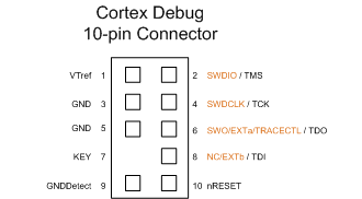
    Normally you have something like this:

    Where VTref is sampled by the debugger (JLink), to match the voltage of the target, which shall be VDD_GPIO in this case.


    Does the module draw any current at all?


    Kind regards,

    Håkon

  • We are using a 6-pin TagConnect with the standard interface from Segger.

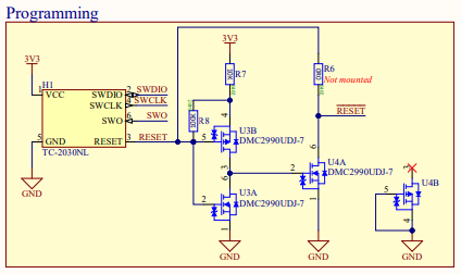
    I have tried both versions here. The version shown where R6 is not mounted, and the version where U4 is removed and R6 mounted.

    Tthe power is 3V3 which is also connected to VDD_GPIO.

  • I have been looking on the reset circuit... Strange as it is copied from the development board.

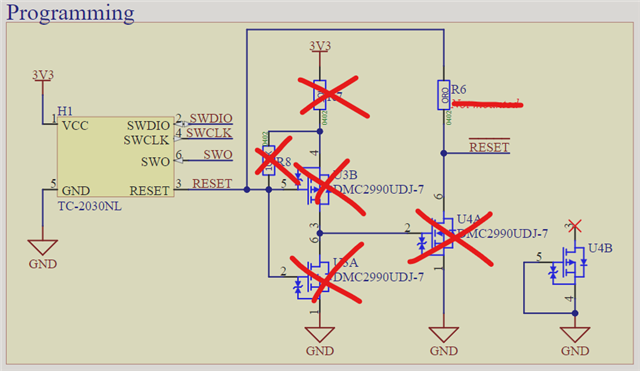
    But it is clearly wrong. I have modified it to look like this:

    So a direct connection from j-link reset to the nReset. There is only the filter with a 1k (R10) and capacitor 100 nF (C12). 

    But I only measure ~ 1V on the reset pin. I have 3V3 on the VDD_GPIO pin. Looking on the data sheet I belive I should measure around 2.2V. It goes to 0V when debugger is disconnected... (VDD_GPIO still at 3V3)

  • Hi,


    Thomas said:
    But I only measure ~ 1V on the reset pin. I have 3V3 on the VDD_GPIO pin. Looking on the data sheet I belive I should measure around 2.2V. It goes to 0V when debugger is disconnected... (VDD_GPIO still at 3V3)

    If it goes to 0V when the debugger is disconnected, it indicates that the nRF9160 is not powered. This pin should be equal to VDD_GPIO

    Have you checked all solderings and connections towards the nRF9160? Specifically the voltages on VDD1/VDD2 etc?


    Kind regards,

    Håkon

  • I have taken a new board as the reset curcuit shown above could have given trouble. Before applying power to the board the whole reset (3 transistors and resistors) were removed.

    I am measureing 3V3 on the VCC_GPIO but no voltage on VDD1, VDD2 or the nRESET pin.

    Soldering looks very good so I do not expect anything like that to be a problem.

    Any suggestion to what I should try?

  • Hi,


    Thomas said:
    but no voltage on VDD1, VDD2 or the nRESET pin.

    If the "VDD_NRF" net shows 0 V, then the net itself is problematic. You will need to check the main power source on your board and see where the problem lies.


    How do you power your board?


    Kind regards,

    Håkon

  • Currently I am powering it using the 5V output from the J-Link, there is a 3V3 regulator on the board. The board is 230V powered normally.

    I am measuring 3V3 from the power supply and on the VDD_GPIO pin. Measured on C7.

    On VDD_NRF net I am measureing 0V or actually 25mV.

    I am measuring this voltage (25mV) on a the involved components and also on both sides of the L1. Also on the ENABLE pin 101.

Reply
  • Currently I am powering it using the 5V output from the J-Link, there is a 3V3 regulator on the board. The board is 230V powered normally.

    I am measuring 3V3 from the power supply and on the VDD_GPIO pin. Measured on C7.

    On VDD_NRF net I am measureing 0V or actually 25mV.

    I am measuring this voltage (25mV) on a the involved components and also on both sides of the L1. Also on the ENABLE pin 101.

Children
No Data
Related