Review PCB design for nrf52840 for Matter or Thread use

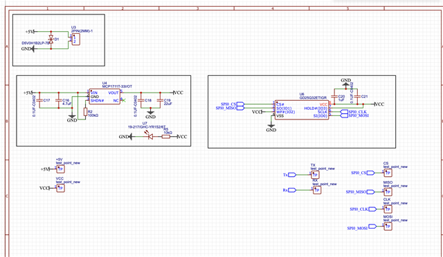
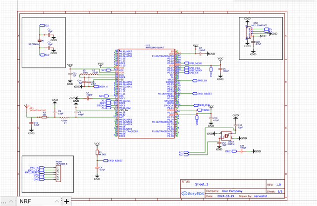
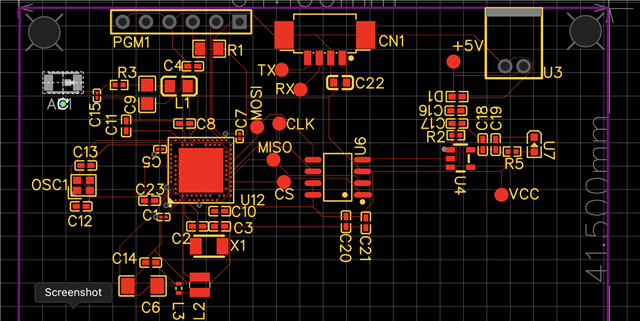
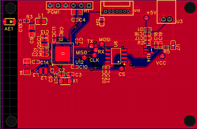
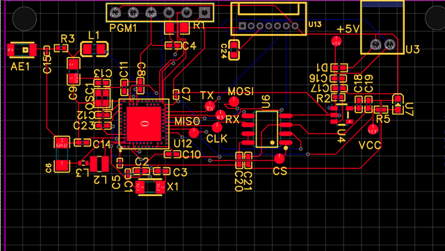
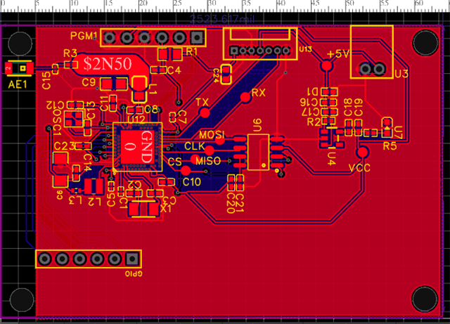
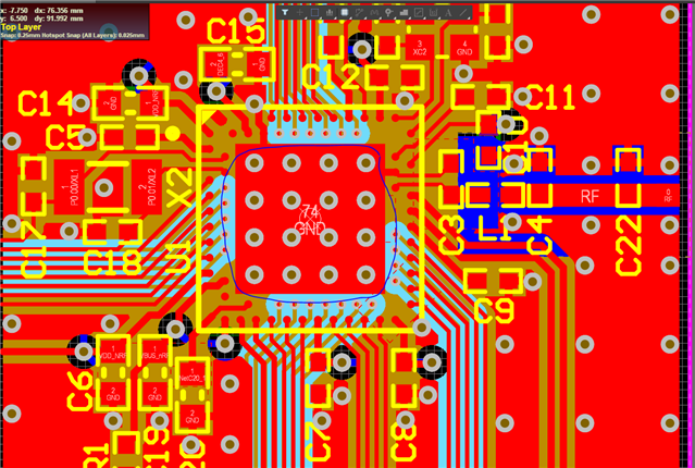
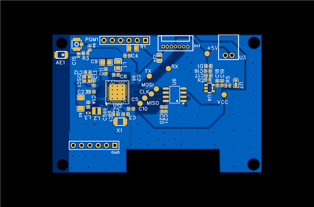
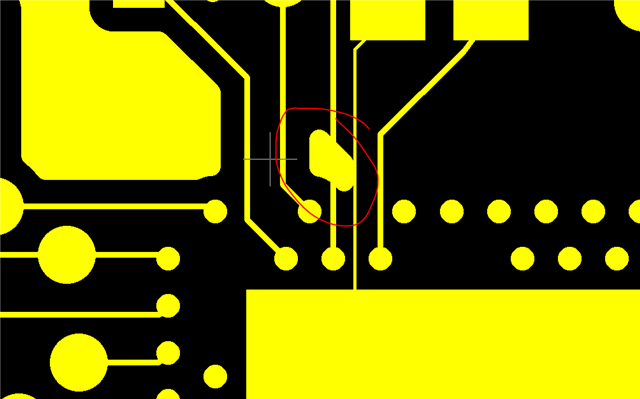
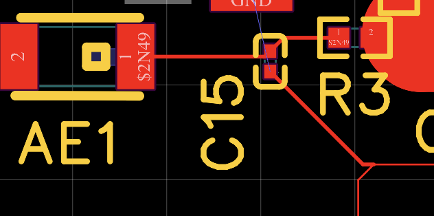
Hi, I am new to PCB design, so I want suggestions for my designed PCB. Please review it once and provide feedback upon that. I am making this PCB to use this with Thread and matter-related products. I have used EasyEda to design the PCB and used the reference designs provided by Nordic. 

 nRF52840 PCB & Antenna Design 

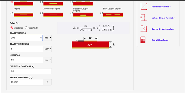
 General PCB design guidelines for nRF52 series 

Parents
  • Hi,

    1. On the SWD header you want to route out VCC not 3V3, so that it follows whatever voltage VCC is at. 
    2. You need a full Pi-network to tune your antenna. Only C15 is not enough. 
    3. DEC4_DEC6 node is connected to the wrong node. It should be over capacitors of the DC/DC components.
    4. You need decoupling on pin A22.
    5. Pullup on Reset pin is not necessary.
    6. What is the internal capacitance of your HFXO and LFXO crystals?

    For the PCB you need to follow the reference design much more closely. Where is your GND layer?

    regards

    Jared 

  • Hi, Thanks for the response, I have updated the design with the Gnd. I will update here after changing the other points you have mentioned . Would you please look into this once and find any improvements


  • I have tried to tune the trace of Antenna as well to 50 ohm , please verify that as well 

  • Hi,

    1. The first capacitor in the matching network should only be grounded to the centerpad, it should not be connected to the rest of the GND layer directly.
    2. It seems that there is a stump, in the matching network, you should remove this.
    3. You need a full matching network the chip antenna.
    4. You need 4x4 vias in the centerpad.
    5. Much more vias in general to stich the GND layer together. 
    6. The transmission line does not look like 50 ohm. 

    regards

    Jared

  • Hi Jared, Thanks for the reply,

    Sorry, but I am not well in understanding the terms that you have used to describe my issue. would please clear bit more in simple.

    1- It should be grounded with centerpad - what does this mean, it is a two-layer PCB?

    2- What does stump mean. ?

    5- Much more vias in general to stick the GND layer together - mean Top and Bottom layers? , and I need to give more vias to connect the ground of the Top and Bottom layers of the copper area?

    6- The transmission line does not look like 50 ohm.  How do you guess that, although I have tried to tune it as I have attached the screenshot, is that incorrect?

  • Hi,

    Sarvesh_dhar said:

    1- It should be grounded with centerpad - what does this mean, it is a two-layer PCB?

    The centerpad, meaning the die ground pad itself needs to be connected to the GND layer by using vias,

    Sarvesh_dhar said:
    2- What does stump mean. ?

    A stump, in this sense is an extension of a wire/transmission line that isn't connected to anything. In the antenna path it's important to avoid stump, because it will move the impedance of the line. I marked the stump with a circle, you should remove it.

    Sarvesh_dhar said:
    5- Much more vias in general to stick the GND layer together - mean Top and Bottom layers? , and I need to give more vias to connect the ground of the Top and Bottom layers of the copper area?

    Yes, in general, the more vias the better as you will make sure that all of GND on your board is on the same potential. 

    Sarvesh_dhar said:
    6- The transmission line does not look like 50 ohm.  How do you guess that, although I have tried to tune it as I have attached the screenshot, is that incorrect?

    It's a guess ,I have not measured it. But if you have based the dimensions on by calculating it to be 50 ohm then it's ok.

    regards

    Jared 

Reply
  • Hi,

    Sarvesh_dhar said:

    1- It should be grounded with centerpad - what does this mean, it is a two-layer PCB?

    The centerpad, meaning the die ground pad itself needs to be connected to the GND layer by using vias,

    Sarvesh_dhar said:
    2- What does stump mean. ?

    A stump, in this sense is an extension of a wire/transmission line that isn't connected to anything. In the antenna path it's important to avoid stump, because it will move the impedance of the line. I marked the stump with a circle, you should remove it.

    Sarvesh_dhar said:
    5- Much more vias in general to stick the GND layer together - mean Top and Bottom layers? , and I need to give more vias to connect the ground of the Top and Bottom layers of the copper area?

    Yes, in general, the more vias the better as you will make sure that all of GND on your board is on the same potential. 

    Sarvesh_dhar said:
    6- The transmission line does not look like 50 ohm.  How do you guess that, although I have tried to tune it as I have attached the screenshot, is that incorrect?

    It's a guess ,I have not measured it. But if you have based the dimensions on by calculating it to be 50 ohm then it's ok.

    regards

    Jared 

Children
Related