Hi there,
I am trying to program my custom board hosting a raytac mdbt53 module (powered by a separate USB cable). I have to use the custom connections in P20 connector for the SWD debugging and flashing. Here are my connections as I have learned from this and this guide:
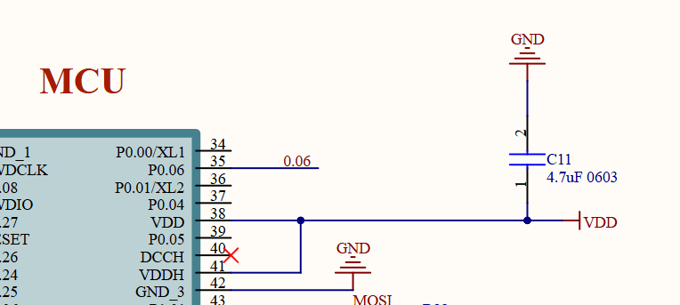
| nRF5340 DK | Custom Board |
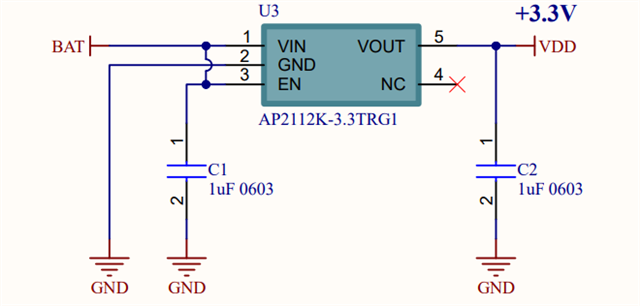
| VTG | VDD |
| VDD nRF | VDD |
| SWDIO | SWDIO (4) |
| SWD CLK | SWD CLK(2) |
| RESET | RESET (6) |
| GND | GND |
There is no GND_DETECT on the v2.0.0 nRF 5340 DK that I am using and therefore I am not able to use that.
On trying to detect the board and program using nRF Connect Desktop, here are the error messages I receive:
11:16:26.119	Selected device with the serial number 001050011532
11:16:26.119	Using nrfutil device to communicate with target via JLink
11:16:26.611	Reading readback protection status for Application core
11:16:26.612	Reading readback protection status for Application core 0%
11:16:26.735	Failed "reading readback protection status for application core". Error: code: 1, description: Generic, message: Batch task protection-get failed, Device error: Setting the debug port SELECT register failed while powering up sys and debug regions (Unknown Error in J-Link DLL (error code =-1)). This might indicate that the debug port is unavailable. Please double-check device power supply and SWD lines, and that SWD isn't disabled
11:16:26.774	Error: Failed with exit code 1. One or more batch tasks failed: * 1050011532: Device error: Setting the debug port SELECT register failed while powering up sys and debug regions (Unknown Error in J-Link DLL (error code =-1)). This might indicate that the debug port is unavailable. Please double-check device power supply and SWD lines, and that SWD isn't disabled (Generic) Message: Batch task protection-get failed, Device error: Setting the debug port SELECT register failed while powering up sys and debug regions (Unknown Error in J-Link DLL (error code =-1)). This might indicate that the debug port is unavailable. Please double-check device power supply and SWD lines, and that SWD isn't disabled.
11:16:26.774	Error: Failed with exit code 1. One or more batch tasks failed: * 1050011532: Device error: Setting the debug port SELECT register failed while powering up sys and debug regions (Unknown Error in J-Link DLL (error code =-1)). This might indicate that the debug port is unavailable. Please double-check device power supply and SWD lines, and that SWD isn't disabled (Generic) Message: Batch task protection-get failed, Device error: Setting the debug port SELECT register failed while powering up sys and debug regions (Unknown Error in J-Link DLL (error code =-1)). This might indicate that the debug port is unavailable. Please double-check device power supply and SWD lines, and that SWD isn't disabled.
In the development version of the custom board, we had an SWD 10 pin connector which worked perfectly. It's only for the custom connections that the flashing does not work anymore.
Kindly advise what could be amiss here. I have already gone through scores of similar posts but none of them are telling any more than what I see in the official documentation.