This post is older than 2 years and might not be relevant anymore
More Info: Consider searching for newer posts

Problem using the nRF52840 to interface an ADS1298 via SPI

Hi DevZone,

I am using the nRF52840 to interface an ADS1298 (ECG Chip) via SPI.

I want to test if the communication between the devices are working by:

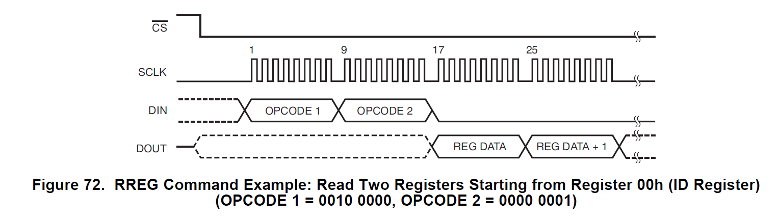
    -  Sending a RREG (Read From Register) opcode from the nRF52840 to the ADS1298

    -  And then read its ID Register.

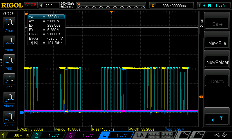
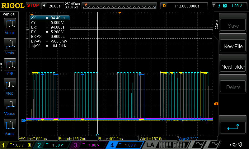
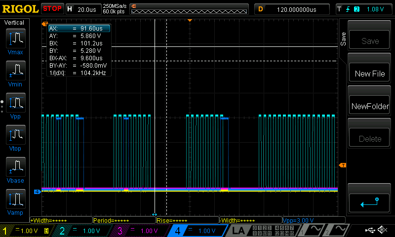
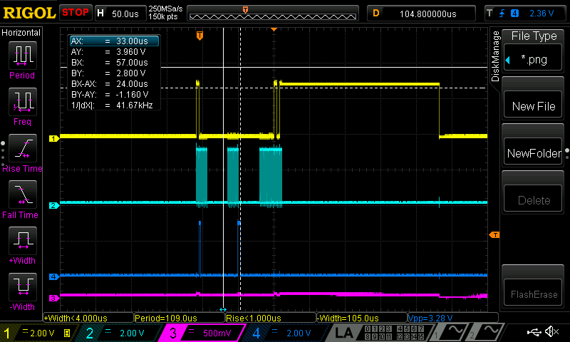
The RREG command is two bytes long, and for multi-byte commands the following needs to be done:

    1.  Send the first byte and then wait for 4 * tCLK  before sending the next byte.

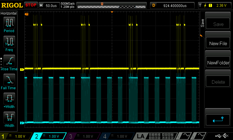
    2. The CS (or SS) pin needs to be held low during the entire session for both transfer and receive.

I am trying to test this with the example provided in the nRF5 SDK 15.3 by using this function:

    -  nrf_drv_spi_transfer(&spi, m_tx_buf, m_length, m_rx_buf, m_length);

My problem is that:

    -  I cannot insert a delay between the bytes when using the nrf_drv_spi_tranfer() for multiple byte transfers

    -  If i use separate calls of the nrf_drv_spi_transfer() for each byte, then the CS pin is not held low.

Is there any way I can use this driver to send multiple bytes with a fixed delay between them, without the CS pin going high during the session?

Thank you for reading

Br. Casper

Parents
  • Update:

    I have found out that I did not wait long enough for VCAP1 to reach a stable value above 1.1V. This takes approx. 2.5 seconds in my setup.

    With this fixed I now have some communication. But I am not getting expected values consistently. Here are some oscilloscope pictures.

    YELLOW = MISO (DOUT on ADS1298R)

    TEAL       = SCLK

    PINK        = /CS

    BLUE      = MOSI (DIN on ADS1298R)

    I think the problem is synchronization related. The way that MISO is left high, almost as if the ADS1298R is expecting more SCLK pulses to finish what it was writing.

    HOWEVER, I have by coincidence found a setting where I get expected values on every second transfer for my read. Here I read the
    ID register and CONFIG1 register as 0xD2 and 0x06 as expected.

    But the initial 1's on the first byte of the SDATAC command are not expected.

    Here is a scope picture of every second attempt to read the registers:

    Has anyone experienced anything similar?

    Thanks for reading,

    Br. Casper 

  • Are you using SPI mode 1 and MSB first? The 'scope pictures are a little unclear, maybe displace the waveforms slightly from each other (vertically) so they are easier to read. This setup works:

        nrf_drv_spi_config_t spi_config = NRF_DRV_SPI_DEFAULT_CONFIG;
        ret_code_t err_code;
    
        spi_config.ss_pin    = ADS_CS_PIN;
        spi_config.miso_pin  = ADS_MISO_PIN;
        spi_config.mosi_pin  = ADS_MOSI_PIN;
        spi_config.sck_pin   = ADS_SCK_PIN;
        spi_config.frequency = NRF_DRV_SPI_FREQ_500K;  // Ensure less than 4 clk cycles for ADS1292
        spi_config.bit_order = NRF_DRV_SPI_BIT_ORDER_MSB_FIRST;
        spi_config.mode      = NRF_DRV_SPI_MODE_1;
        APP_ERROR_CHECK(nrf_drv_spi_init(&mAfeSpiInstance, &spi_config, afe_spi_event_handler, NULL));

    However as you are going off-board with the signals, I would suggest start with enhanced drive on SCK, MOSI and CS. The traces above may look clean, but fast jitter on the edges are not visible at this 'scope resolution, and edge jitter can corrupt expected transactions, notably on SCK. Add this after spi init:

       // High power output pins to ensure clean edge transitions off-board
       nrf_gpio_cfg(ADS_SCK_PIN
                    NRF_GPIO_PIN_DIR_OUTPUT,
                    NRF_GPIO_PIN_INPUT_DISCONNECT,
                    NRF_GPIO_PIN_NOPULL,
                    NRF_GPIO_PIN_H0H1,       // Test with High Drive high and low level
                    NRF_GPIO_PIN_NOSENSE);

  • Hi hmolesworth,

    Thank you for replying!

    Yes, I am using MSB first and SPI_MODE_1 (CPOL = 0 and CHPA = 1).

    I tried using the enhanced drive setting you suggested, but sadly, it does not change the behavior.

    I have also tried using up to a 120Ohm resistor in series with the SCLK pin, added as close as possible to the source.

    I have taken further snapshots with the oscilloscope:

    YELLOW: MISO

    TEAL: SCLK

    BLUE: MOSI

    PINK: Not connected

    The first picture is without the 120R in series with SCLK. At first glance it seems as if noise on SCLK triggers a response from the ADS1298R. The noise on the SCLK pin (teal) on the first snapshot is significantly reduced by the 120R resistor. 

    I then added the 120R to the SCLK pin. Then I waited until I noticed an unexpected output from the ADS1298R on the MISO pin and took a snapshot again. The changes in MISO and SCLK line up here.

    (EDIT: Second snapshot was uploaded twice, and was changed to correct zoomed in snapshot).

    BUT, when I zoomed in as on the third snapshot it looks more like  the noise on MISO, (Yellow) is not induced by the SCLK pin (Teal).

    I think this, because the level-change on MISO (Yellow) is not being triggered by the peak voltage of the noise on the SCLK (Teal), but was already changing earlier than the peak.

    I do not think that it is a SCLK pin specific problem with the noise, but I do suspect that noise could be the issue. Does anyone have any further suggestions to how I should proceed looking for the issue here?

    Br. Casper

Reply
  • Hi hmolesworth,

    Thank you for replying!

    Yes, I am using MSB first and SPI_MODE_1 (CPOL = 0 and CHPA = 1).

    I tried using the enhanced drive setting you suggested, but sadly, it does not change the behavior.

    I have also tried using up to a 120Ohm resistor in series with the SCLK pin, added as close as possible to the source.

    I have taken further snapshots with the oscilloscope:

    YELLOW: MISO

    TEAL: SCLK

    BLUE: MOSI

    PINK: Not connected

    The first picture is without the 120R in series with SCLK. At first glance it seems as if noise on SCLK triggers a response from the ADS1298R. The noise on the SCLK pin (teal) on the first snapshot is significantly reduced by the 120R resistor. 

    I then added the 120R to the SCLK pin. Then I waited until I noticed an unexpected output from the ADS1298R on the MISO pin and took a snapshot again. The changes in MISO and SCLK line up here.

    (EDIT: Second snapshot was uploaded twice, and was changed to correct zoomed in snapshot).

    BUT, when I zoomed in as on the third snapshot it looks more like  the noise on MISO, (Yellow) is not induced by the SCLK pin (Teal).

    I think this, because the level-change on MISO (Yellow) is not being triggered by the peak voltage of the noise on the SCLK (Teal), but was already changing earlier than the peak.

    I do not think that it is a SCLK pin specific problem with the noise, but I do suspect that noise could be the issue. Does anyone have any further suggestions to how I should proceed looking for the issue here?

    Br. Casper

Children
Related