This post is older than 2 years and might not be relevant anymore
More Info: Consider searching for newer posts

GPIO setup parameters for AoA Antenna switching

I have an issue with getting the I/Os correctly setup for antenna switching.

I am running the radio_test example code with the following modifications. 

So far, I have the following code for the GPIO setup:

//Defines are at top of file
#define ANT1 NRF_GPIO_PIN_MAP(0,17)
#define ANT2 NRF_GPIO_PIN_MAP(1,8)
#define ANT3 NRF_GPIO_PIN_MAP(1,7)
#define ANT4 NRF_GPIO_PIN_MAP(1,6)

//other support code

//Pin config
nrf_gpio_pin_clear(ANT1);
nrf_gpio_cfg_output(ANT1);
nrf_gpio_pin_clear(ANT2);
nrf_gpio_cfg_output(ANT2);
nrf_gpio_pin_clear(ANT3);
nrf_gpio_cfg_output(ANT3);
nrf_gpio_pin_clear(ANT4);
nrf_gpio_cfg_output(ANT4);

//DFE pin config
NRF_RADIO->PSEL.DFEGPIO[0] = ANT1; //(P0.17)
NRF_RADIO->PSEL.DFEGPIO[1] = ANT2; //(P1.08)
NRF_RADIO->PSEL.DFEGPIO[2] = ANT3; //(P1.07)
NRF_RADIO->PSEL.DFEGPIO[4] = ANT4; //(P1.06)

NRF_RADIO->SWITCHPATTERN = 1; //Only P0.07 active
NRF_RADIO->SWITCHPATTERN = 2; //Only P1.08 active
NRF_RADIO->SWITCHPATTERN = 4; //Only P1.07 active
NRF_RADIO->SWITCHPATTERN = 8; //Only P1.06 active

NRF_RADIO->DFEMODE = RADIO_DFEMODE_DFEOPMODE_AoA;
NRF_RADIO->DFECTRL1 = 10 << RADIO_DFECTRL1_NUMBEROF8US_Pos | 
                       1 << RADIO_DFECTRL1_DFEINEXTENSION_Pos;

Then in the radio_test.c file, I include in the function radio_rx( ...)

uint32_t g_iq_packet[RADIO_MAX_PAYLOAD_LEN];

void radio_rx(....)
{
//orig example code still exists here, only not shown
    NRF_RADIO->DFEPACKET.PTR = (uint32_t)g_iq_packet;

}

From a board running the radio_test example, I issue the 'start_tx_modulated_carrier' command the immediately issue the 'start_rx" command on a seperate DK also running the radio_test example with the above modifications.

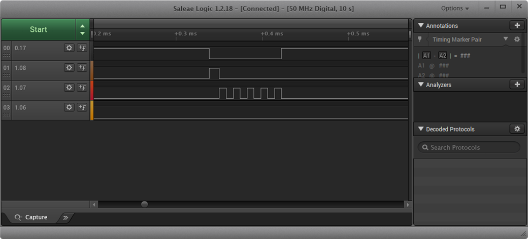
I expected to see a short duration square wave on each of the antenna GPIO pins, so, 4 square waves cascading in time. However from my logic analyzer capture, you can clearly see that is not the case.

How should I be setting up the config registers to fire each of the pins.  Nothing else is connected to the board except the logic analyzer.

Also, how do I correlate the IQ data from the DFEPACKET.PTR to the specific antenna?

  • Hi Dmitry,

    Thanks. What mode (1Mbps or 2Mbps) are you using? I'm confused, as the phase must surely cycle over either 4us for a 250 kHz tone (1Mbps mode) or 2us for a 500 kHz tone (2Mbps mode). Or, with 0.125us sampling, 32 samples for 1Mbps or 16 samples for 2Mbps mode. Where does 8us come from?

    Your phase changes are much cleaner than mine. My phase phase looks like this, which I've posted in a new question: 

    My RF switch ought to be fast enough. Something is not right.

  • Hi Pete,

    I'm using 1Mbps, one of my boards seems to have low-quality crystal (a -50ppm error would give -120kHz frequency offset at 2.4Ghz, that's near my case).

    From your diagram, your switching time is about 1.2 usec, that's sufficient even for 2usec switching period - I don't see any problem here. Check whether you've set controlling GPIOs to high-drive mode.

  • Pete,  for what its worth, I see stuff similar to you. What is your hardware setup?

  • Hi ,

    One more thing related with mapping of antennas to samples. In all diagrams there is an information that after reference period there is a switch-slot/sample-slot pairs sequence. Unfortunately there is a gap. The gap lasts for single switch-slot. So first sample you receive is taken in first sampling-slot. After that each sample is stored in configured delay. 

    That does matter for mapping of antennas to samples, especially in case of oversampling. 

    Let take for example following settings:

    • NUMBEROF8US=3 ->24us
    • TSWITCHSPACING=2us
    • TSAMPLESPACING=250ns
    • TSAMPLESPACINGREF=250ns

    Number of samples would be: Ref period 8us/0.25 = 32, switch-period 12/0.25=48

    First sample from switch-period would be taken in first sampling slot, so you would have a time delay of 4 samples (1us - swtich slot).

    After that delay you would have samples: 

    • 4 samples taken in 1st sampling-slot (antenna 1)
    • 4 samples taken in 2nd switch-slot (antenna 2)
    • 4 samples taken in 2nd sampling-slot (antenna 2)
    • 4 samples taken in 3rd switch-slot (antenna 3)

    As said in quote, Is it correct to say that first sample after reference period aligns to first sampling slot. so there will be 1us delay(switch slot time = switch spacing/2) for first sample after reference period?

    If so than in out of 12us switching-sampling period only 11us will be samples so there will be 11/0.25 = 44 samples only instead of 48 as said in above quote. Am I correct?

    But actually I am getting 48 samples with this setting what is correct understanding regarding switching pattern and sampling order with respect to it.

Related