Hello,
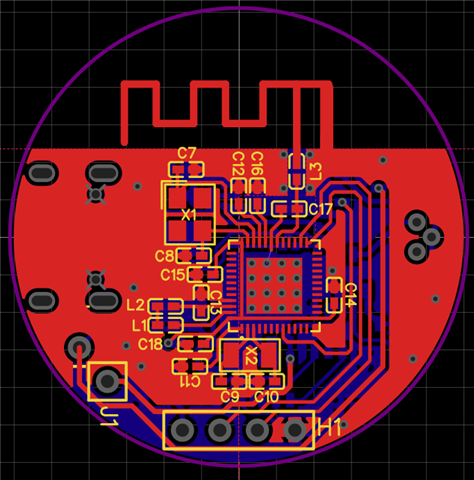
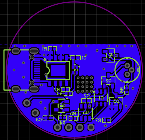
I have designed my own custom NRF52840 board for my own apllication. I tried to gather as much information about the NRF as possible and put it in an schematic. I am building the PCB in EASYEDA but first i want to make sure the schematics are right. The purpose of the PCB is to control an laser diode by an smartphone app using the BLE network of the SoC. The schematic consist of 2 sheets and i will try to explain everything as good as possible.
Sheet 1: (Power supply)
USB-C Connector: The board is going to be charged and programmed by an USB-C cable.
Battery Charging: The PCB is powered by an 3.7V LiPo battery which is charged via the TP4056 IC.
Battery Protection: The LiPo is protected by the DW01 and FS8205.
Vin -> 3.3V: The battery voltage is converted to 3.3V (VDD) for the NRF52840 by the NCP114.
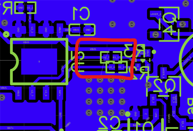
Laser Diode: The laser diode is powered by an constant current circuit.
Battery: Solder pads for the battery.
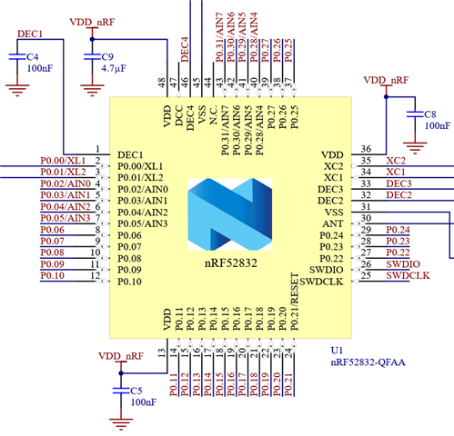
Sheet 2 (Controller):
USB -> UART: The CP2104 is used to program the NRF52840 by an USB cable.
Crystals: The crystals for the NRF52840
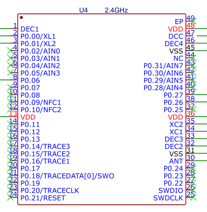
NRF52840: The SoC itself.
I have a couple questions about this project:
- Are my power nets designed the right way ?
- Is the NRF52840 going to work like this ?
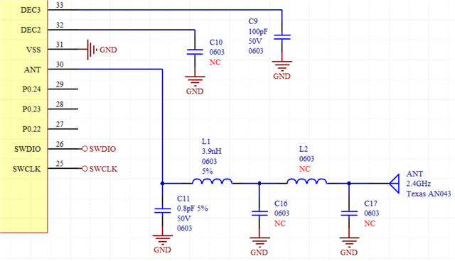
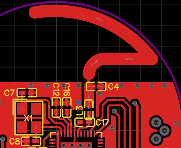
- I connected the ANT pin untill the antenna itself. I need to look further into this which antenna is good for this project but maybe somebody can already help me with this ?
- Maybe my biggest question of this whole project. This PCB is eventually going to be mass produced after the prototypes are tested and fully working. What is the best way to program a board like this when its going to be mass produced. I saw somebody do it this way and i liked it because it uses the USB port. But i also saw that they use the SWDIO and SWDCLK pins but i dont know a lot about this. Can somebody help me with this ?
- Final question. Are there any other upgrades i can make for this schematic ?