low power wearable electronics.

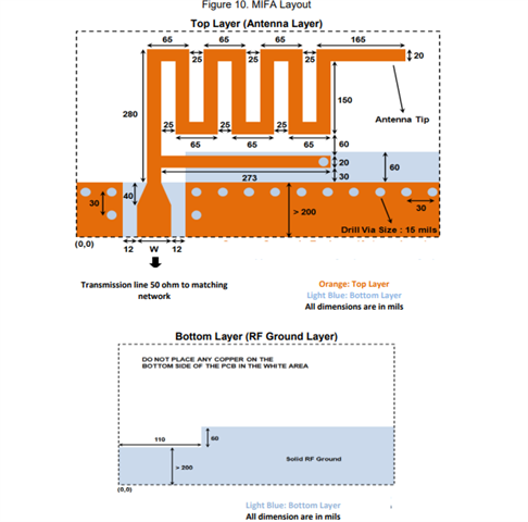
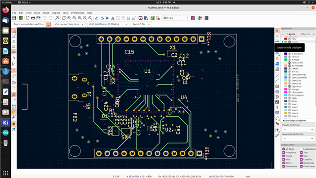
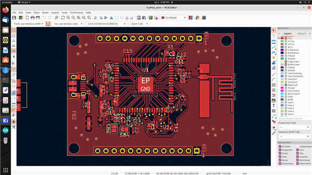
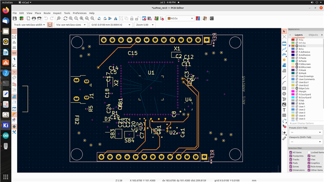
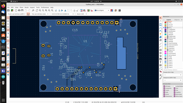
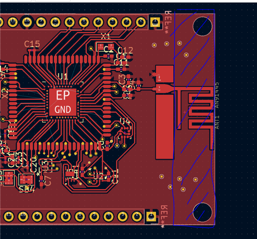
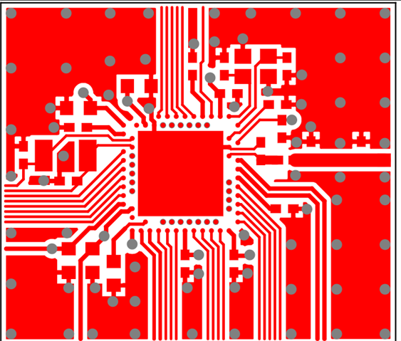
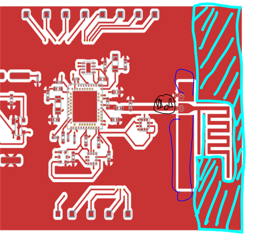
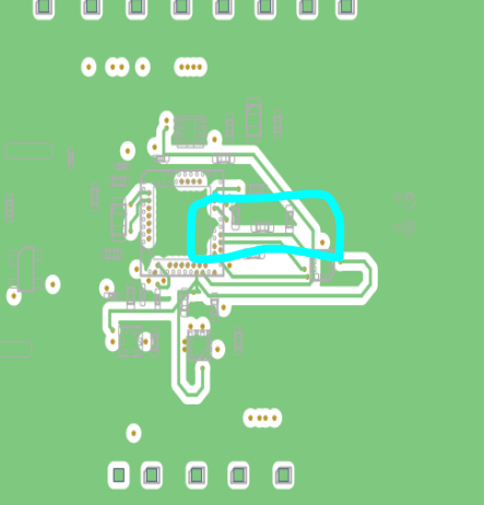
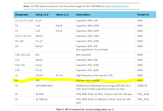
I have designed single layer pcb for the first time using kiCAD software for  low power (1-5mW) wearable electronics using nRF52840,one accelerometer sensor i.e.BMA400,one recommended antenna(AN91445) and one 2x5 programming port. Please refer to the attached the document. Please suggest any correction and a suitable program/code so that we can test it using ARM Segger Studio.Low power basic Reference.pdfLow power basic1.0.csv

Parents
  • Hi  ,
    The cost saving is not worth it in this case. The performance will be terrible and not representative of a two(multi) layered design so it will not be representable of the final product. 

    So this is not recommended. Pleas follow the reference layout to achieve good results. Failing to follow the design guidelines can result in a non working device. 

    The center pad of the SoC needs to be connected to the rest of the ground for the radio to work as intended. 

    Also the antenna you have used is degined to have a ground plane also. So it might not work at all as it is in your current desing.


    https://www.infineon.com/dgdl/Infineon-AN91445_Antenna_Design_and_RF_Layout_Guidelines-ApplicationNotes-v09_00-EN.pdf?fileId=8ac78c8c7cdc391c017d073e054f6227 

    Regards,
    Jonathan

  • This is the updated version of Low Power Wearable Electronics.Please check it and suggest corrections....

  • Hi,

    There needs to be a cutout area for the antenna. 


    Move the critical component closer to the nrf52 SoC. Use our ref design as a guide here and try to copy exactly. Here is a showcase https://infocenter.nordicsemi.com/topic/ps_nrf52840/ref_circuitry.html?cp=5_0_0_6_2_15#layout 


    See the response I have here : https://devzone.nordicsemi.com/f/nordic-q-a/98199/matching-network-placement-and-routing-ble-antenna-routing  It includes some links to some guides that have more info. 


    Regards,
    Jonathan

  • How to use TWIM for reading and writing data from an external sensor with nrf5340dk.

    My target is to read and write data from a sensor using bare metal programming for the nrf5340dk with minimum power consumption.

    I had a problem with this program. Though the program does not give any error, it seems to be unable to read data from the sensor.

    Our program code is given below:

    #include "nrf.h"


    //SCL & SDA LINES
    #define PIN_SCL           3
    #define PIN_SDA           4
    #define PORT_NO           1

    #define SLAVE_ADDRESS     0xDF

    // Definitions for delay function
    #define SYSTICK_LOAD_VALUE  64000  // for each ms
    #define CTRL_ENABLE (1U << 0)
    #define CLK_SOURCE (1U << 2)
    #define CTRL_COUNTFLAG (1U << 16)
    // Delay function
    void delay(int delay) {
        // Load the number of clock cycles per millisecond
        SysTick->LOAD = SYSTICK_LOAD_VALUE;
        // Clear SysTick current value register
        SysTick->VAL = 0;
        // Enable SysTick and select processor clock source
        SysTick->CTRL = CTRL_ENABLE | CLK_SOURCE;

        for (int i = 0; i < delay; i++) {
            // Wait until the count flag is set
            while ((SysTick->CTRL & CTRL_COUNTFLAG) == 0) {}
        }
        SysTick->CTRL = 0;
    }


    void gpioEnable(void){
      NRF_P1_S -> PIN_CNF[PIN_SCL] =  (GPIO_PIN_CNF_PULL_Pullup << GPIO_PIN_CNF_PULL_Pos) |
                                      (GPIO_PIN_CNF_DRIVE_S0D1 << GPIO_PIN_CNF_DRIVE_Pos) |
                                      (GPIO_PIN_CNF_MCUSEL_Peripheral << GPIO_PIN_CNF_MCUSEL_Pos);
      NRF_P1_S -> PIN_CNF[PIN_SDA] =  (GPIO_PIN_CNF_PULL_Pullup << GPIO_PIN_CNF_PULL_Pos) |
                                      (GPIO_PIN_CNF_DRIVE_S0D1 << GPIO_PIN_CNF_DRIVE_Pos) |
                                      (GPIO_PIN_CNF_MCUSEL_Peripheral << GPIO_PIN_CNF_MCUSEL_Pos);
    }

    void i2cEnable(void){
      NRF_SPIM1_S -> ENABLE = (SPIM_ENABLE_ENABLE_Disabled << SPIM_ENABLE_ENABLE_Pos);
      NRF_SPIS1_S -> ENABLE = (SPIS_ENABLE_ENABLE_Disabled << SPIS_ENABLE_ENABLE_Pos);
      NRF_TWIS1_S -> TASKS_STOP = (TWIS_ENABLE_ENABLE_Disabled << TWIS_ENABLE_ENABLE_Pos);
      NRF_UARTE1_S -> ENABLE = (UARTE_ENABLE_ENABLE_Disabled << UARTE_ENABLE_ENABLE_Pos);
      NRF_TWIM1_S -> ENABLE = (TWIM_ENABLE_ENABLE_Enabled << TWIM_ENABLE_ENABLE_Pos);
    }

    void i2cDisabled(void){
      NRF_TWIM1_S -> ENABLE = (TWIM_ENABLE_ENABLE_Disabled << TWIM_ENABLE_ENABLE_Pos);
    }
    void i2cConfig(){
    //The SCL and SDA signals are mapped to physical pins using the PSEL.SCL and PSEL.SDA registers.
    //PSEL.SCL and PSEL.SDA must only be configured when the TWI master is disabled.
      NRF_TWIM1_S -> PSEL.SCL = (PIN_SCL << TWIM_PSEL_SCL_PIN_Pos) |
                                (PORT_NO << TWIM_PSEL_SCL_PORT_Pos) |
                                (TWIM_PSEL_SCL_CONNECT_Connected << TWIM_PSEL_SCL_CONNECT_Pos) ;
                                
      NRF_TWIM1_S -> PSEL.SDA = (PIN_SDA << TWIM_PSEL_SDA_PIN_Pos) |
                                (PORT_NO << TWIM_PSEL_SDA_PORT_Pos) |
                                (TWIM_PSEL_SDA_CONNECT_Connected << TWIM_PSEL_SDA_CONNECT_Pos);
      NRF_TWIM1_S -> FREQUENCY = (TWIM_FREQUENCY_FREQUENCY_K100 << TWIM_FREQUENCY_FREQUENCY_Pos);
    }

    int i2cRead(uint8_t slave_addr, uint8_t mem_addr, uint8_t *data){
      //volatile int tmp;
      NRF_TWIM1_S -> TASKS_STARTRX = (TWIM_TASKS_STARTRX_TASKS_STARTRX_Trigger << TWIM_TASKS_STARTRX_TASKS_STARTRX_Pos);
      while (!(NRF_TWIM1_S -> EVENTS_RXSTARTED & 1)){};
      NRF_TWIM1_S -> ADDRESS = (slave_addr << TWIM_ADDRESS_ADDRESS_Pos);
      while (!(NRF_TWIM1_S -> ERRORSRC & 2)) {};
      NRF_TWIM1_S -> ADDRESS = (mem_addr << TWIM_ADDRESS_ADDRESS_Pos);
      while (!(NRF_TWIM1_S -> EVENTS_RXSTARTED & 1)){};
      NRF_TWIM1_S -> RXD.PTR = (uint32_t)&data;
      NRF_TWIM1_S -> RXD.MAXCNT = sizeof(data);
      NRF_TWIM1_S -> TASKS_STARTRX = (TWIM_TASKS_STARTRX_TASKS_STARTRX_Trigger << TWIM_TASKS_STARTRX_TASKS_STARTRX_Pos);
      while(!(NRF_TWIM1_S -> EVENTS_LASTRX & 1)){};
      NRF_TWIM1_S -> TASKS_STOP = (TWIM_TASKS_STOP_TASKS_STOP_Trigger << TWIM_TASKS_STOP_TASKS_STOP_Pos);
      NRF_TWIM1_S -> EVENTS_LASTRX = 0;
      return (int) (*data);
    }

    int main(){
      int a;
      i2cDisabled();
      gpioEnable();
      i2cConfig();
      i2cEnable();
     
      while (1){
        a = i2cRead(SLAVE_ADDRESS, 0,(uint8_t*) &a );
        printf("The data read is : %d", a);
        delay(1000);
        
      }
      return 0;
    }

  • Is there any reason for this, that all critical components should be close to the chip....?
Reply Children
Related