Jitter in high priority thread loop with irq_lock and k_sched_lock

I've been working on a custom device utilising the nRF52832 that needs to switch GPIOs in tightly controlled pulses. The problematic section is part of a much larger project written using nRF Connect SDK v2.6.1:

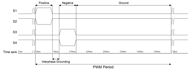
k_sched_lock();
key = irq_lock();
positive_electrodes();
k_busy_wait(50);

float_electrodes();
k_busy_wait(40);

negative_electrodes();
k_busy_wait(50);

ground_electrodes();
irq_unlock(key);
k_sched_unlock();   

k_usleep(10e3);

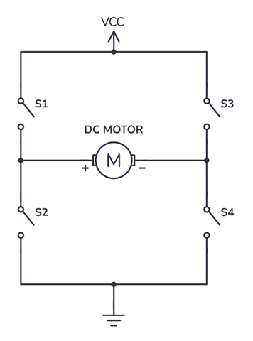
The code block is the body of an infinite while loop in a thread function. The thread priority is 1 (higher than every other created thread). The positive_electrodes, float_electrodes, negative_electrodes, and ground_electrodes functions are just wrappers around a series of log and gpio_pin_set_dt statements.

I am checking the GPIO waveforms on an oscilloscope, I would expect to see pulses that are 50us and 40us long. This is mostly what I see, however, every other second or so, I see a jump on the pulse width with a maximum of 190us when it should be 50us.

Pulse width jitter has been a major problem in previous versions of my software, that I drastically reduced by utilising k_busy_wait instead of k_usleep, and by adding the irq_lock. However, the jitter has not disappeared. Based on a sample size of 1000 pulses, the deviation for each of the 50us pulses I am scoping is about 10us, which is a lot higher than I would expect. 

Does anyone have any ideas of what could be causing the occasional extremely long pulses despite all the mitigation I have tried (irq_lock, k_sched_lock, highest priority thread)? I have tried moving from the thread based implementation to a chain of timers that start the next one on expiry but that just exacerbated the jitter beyond reason. 

Edit: I forgot to mention that while I extensively use the logging module, logging is turned off in the project config file since we have to way of interfacing with the MCU once in production.

Parents
  • Was there a reason to not just use hardware PWM to drive the GPIO? The pulses would then have no jitter; if code is required for each part of the pulse or some parts of the pulse the EGU could be used to generate interrupts which would handle any semaphores and the like; no need for thread interaction for the actual pulse timing.

    Maybe share the driving circuit for the electrodes; a 4-output PWM can control the Pos-Float-neg-ground phases by selectively setting each of the 4 outputs to (say) H1D0, D1D0, H0D1, H1D0 but need to see how the outputs are driven to confirm. It is possible to use more than one PWM synchronously with 0nSec phase delay as well as no jitter. I provide an example here; the nRF52832 is simple but the changed PWM implementation on the nRF52833 required slightly different code: pwm-anomaly-nrf52832-vs-nrf52833 and start-pwms-synchronous

  • The driving circuit is an H-bridge (I've pasted a dummy setup I found online; my circuit does not connect to a motor). I have 4 GPIOs going to the 4 switch inputs on the H-bridge arms. These signals have line buffers to avoid overloading the GPIOs.

    So when I call positive_electrodes(), S1 and S4 turn on. Similarly, when I call ground_electrodes(), S2 and S4 are turned on. I used 50us and 10ms times as examples in the code excerpt but I actually need to configure pulse widths between 50us - 500us delivered at 10Hz - 200Hz at runtime based on user input. 

    My initial idea when developing this system was to use PWM, but two channels are spoken for already. Plus, I needed the positive and negative pulses to be delivered successively with no overlap. As far as I know there aren't ways to implement a phase delay between two pins on the same PWM channel (at least in the NCS Zephyr APIs that I've checked). 

    Thanks for linking those threads, I took a look and they definitely are interesting. I haven't interacted with the PPI or EGU so I'll do some homework to see if those could imply a solution. Thanks!

  • Only 2 pins are required to drive the H-bridge (1 for S1,4 and 1 for S2,3) if using external logic though 4 pins are preferred for hardware simplicity, and the most important issue is usually to ensure that there is a way to control the dead band (non-overlap) as the drive voltages are not square waves as shown on (say) a logic analyser but instead exponential or linear ramps on both rising and falling edges. Overlap due to thresholds and sloping signals crossing can be catastrophic (shorted motor drivers exploding) or simply a nuisance (unwanted battery power loss). Here are some examples I provided for H-Bridge PWM with dead-bands; might be helpful:

    pwm-interrupts

    how-to-set-up-pwm-dead-time-at-the-end-of-period

  • I posted an example showing how you can use the nrfx pwm driver in the nRF Connect SDK here:  RE: Softblink in NCS/Zephyr .  

  •  It was about time I looked deeper than what the Zephyr APIs offer and I am thoroughly impressed by how powerful the PWM, PPI, and TIMER peripherals seem to be. I have an idea that I'd like your opinion on.

    Turns out, if I slightly modify my output signal chain to positive -> GND -> negative -> GND, S2 = ~S1 and S4 = ~S3. Since the frequency and duty cycle is the same across all 4 (ignoring dead time for now) with S3 and S4 just being phase shifted by a known amount, I figured I could use my remaining PWM module to get the signals made. But if I understand correctly based on the PWM documentation and this discussion post, triggering TASKS_SEQSTART[n] will start the wave counter for every enabled channel and so I will not be able to use PPI to generate a PWM phase delay for channels within a PWM module, only from one PWM module to the other, correct?

    If that is indeed the case, how about I setup S1 and S2 as 2 channels of the remaining PWM module operating with an up-and-down wave counter and have S3 and S4 as GPIOTE pins? This way I could set the S2 duty cycle to be slightly larger so I get deadtimes on either side of the S1 enable region. 

    EVENTS_SEQSTARTED[0] can then be used to start a TIMER that is already configured with the appropriately calculated CC[n] registers such they can trigger the 4 GPIOTE SET and CLR tasks that are required to form the negative phase and transition into the GND phase for the rest of the PWM period.

    The only other issue I can think of is that EVENTS_SEQSTARTED[0] is only raised at the very start of the PWM module being started, but this can be solved by another TIMER that lasts exactly as long as the PWM period to restart the S3/S4 GPIOTE triggering TIMER.

    Would this then in-fact be an exclusively hardware implementation to drive the H-bridge? Of course every time the user changes the pulse width/pulse frequency I should be able to stop the PWM and clear, reset all the timers, and reconfigure PWM and TIMER registers for the new settings.

    Also,  thanks for linking that example, it helped me understand how I should approach writing this up.

    Please let me know whether this vague plan seems feasible to either of you or if I have a critical misunderstanding of the peripherals.

  • Much simpler solution is to simply use all 4 PWM output pins and no GPIOTE would then be required; a true hardware solution. I have some code which does just this, used as a pulse driver for a pump motor. There are two sequences in the PWM peripheral allowing toggling between sequences which allows the user to change pulse width and pulse frequency without stopping or interrupting the pulse train. Usually with a fixed Dead Band ("Interphase Grounding") only the pulse frequency is changed and the pulse widths auto-scale; in some cases the pulse frequency is kept constant and the pulse widths are changed allowing power control (think LED dimming). Both are possible with the PWM peripheral. Conceptually using 2 pins with external hardware looks like this (one table for each sequence):

    //  Full or Half H-Bridge PWM - Variable pulsewidth/pulse frequency step lengths
    //
    //   +----------------------------------> COMP0 OUT[0] Compare 0 - PIN_PWM_S1S4
    //   |         +------------------------> COMP1 OUT[1] Compare 1 - PIN_PWM_S2S3
    //   |         |         +--------------> COMP2 OUT[2] Compare 2 - PIN_SUPPLY_EN (3 volt power source)
    //   |         |         |               (COMP3 OUT[3] Compare 3 not used)
    //   |         |         |
    // +---------+---------+---------+---------+
    // | Compare | Compare | Compare | Top     | Cycle N
    // +---------+---------+---------+---------+
    // | Compare | Compare | Compare | Top     | Cycle N+1
    // +---------+---------+---------+---------+
    // | Compare | Compare | Compare | Top     | Cycle N+2
    // +---------+---------+---------+---------+
    //                                 |
    //                                 +----> COUNTERTOP Cycle Period 4 steps, 1MHz clocks. Range 3-32767
    //                                       (LOOP       Repeat Count, number of periods - no repeats)
    

    Using 4 pins requires other than Wave Mode or requires two PWM peripherals in synch. I'll dig out my code and post later today.

Reply
  • Much simpler solution is to simply use all 4 PWM output pins and no GPIOTE would then be required; a true hardware solution. I have some code which does just this, used as a pulse driver for a pump motor. There are two sequences in the PWM peripheral allowing toggling between sequences which allows the user to change pulse width and pulse frequency without stopping or interrupting the pulse train. Usually with a fixed Dead Band ("Interphase Grounding") only the pulse frequency is changed and the pulse widths auto-scale; in some cases the pulse frequency is kept constant and the pulse widths are changed allowing power control (think LED dimming). Both are possible with the PWM peripheral. Conceptually using 2 pins with external hardware looks like this (one table for each sequence):

    //  Full or Half H-Bridge PWM - Variable pulsewidth/pulse frequency step lengths
    //
    //   +----------------------------------> COMP0 OUT[0] Compare 0 - PIN_PWM_S1S4
    //   |         +------------------------> COMP1 OUT[1] Compare 1 - PIN_PWM_S2S3
    //   |         |         +--------------> COMP2 OUT[2] Compare 2 - PIN_SUPPLY_EN (3 volt power source)
    //   |         |         |               (COMP3 OUT[3] Compare 3 not used)
    //   |         |         |
    // +---------+---------+---------+---------+
    // | Compare | Compare | Compare | Top     | Cycle N
    // +---------+---------+---------+---------+
    // | Compare | Compare | Compare | Top     | Cycle N+1
    // +---------+---------+---------+---------+
    // | Compare | Compare | Compare | Top     | Cycle N+2
    // +---------+---------+---------+---------+
    //                                 |
    //                                 +----> COUNTERTOP Cycle Period 4 steps, 1MHz clocks. Range 3-32767
    //                                       (LOOP       Repeat Count, number of periods - no repeats)
    

    Using 4 pins requires other than Wave Mode or requires two PWM peripherals in synch. I'll dig out my code and post later today.

Children
  • If I understand correctly, the snippet you posted requires tying S1/S4 on one pin, and S2/S3 on another? 

    The GND phases I refer to above aren't dead times, those are specifically when both low side switches (S2/S4) are turned on so that the positive and negative terminals of the output are both pulled to ground. This is a necessary part of the output terminal behaviour. Do you still think this could be solved by one PWM module? 

    Both other modules are spoken for: one for a 4kHz buzzer and another the control signal for a boost converter. 

Related