nRF9151 Low Power Mode.

I am using the nRF9151 DK, using the Serial LTE Modem firmware from the nRF Connect quick start.

I am planning to use nRF9151 as a serial modem, and connect it to my Host MCU using UART.

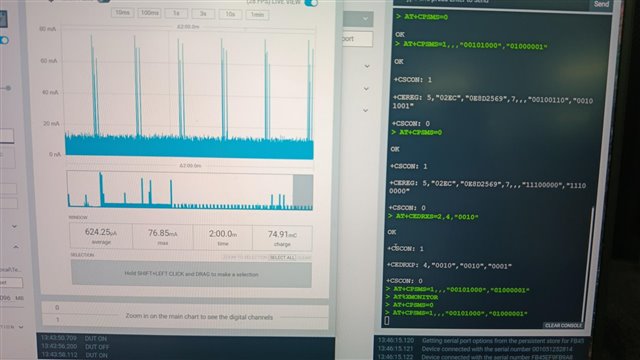
I am using the Power Profile II to measure the current of VDD_nRF.

Questions:

  1. Is this the product code that I should be using for my final product?
  2. Power save mode:
    1. I set the modem LPM. The average current is about 500uA in LPM. Why is it still so high? What is nRF9151 drawing current for? Is it because nRF9151 UART is still enabled?
    2. I press button 1 on the DK, the average current went down to 3uA.
    3. I press button 1 again, it seems to wake the nRF9151 up, with average current about 500uA again, but I lost all network configurations.
    4. Questions:
      1. What does button 1 do exactly? Any documents that describe exactly what it does?
      2. What is the proper way to go into deep power save mode, assuming I am using this Serial LTE Modem firmware in my final product?
      3. Is there a even lower power mode that the button 1 method? i.e. average current < 1uA maybe?
  3. There are some instances, when I leave the DK alone for maybe 10 mins, then I tried to send a AT command, the DK is not responsive in the sense it did not send back "OK" or network messages. However, my AT command was executed (based on the current profile of the Power Profiler II). Is this a know issue? Below image shows this error. In the image, bottom right, a few AT commands are sent but there were not response received.

  • Hi! Simon,

    I tried the chat bot. Didn't return the answer I needed.

    I will be trying '"serial_modem_v0.3.0_nrf9151dk_ext_mcu.hex', and I understand I need to follow the pin definition documented here. I will be connecting these pins to external MCU. If I disable nRF9151 by pulling the ENABLE pin low, will the external MCU connections to nRF9151 pins (UART and GPIOs) damage the chip? What is the state of the nRF9151 pins (UART and GPIOs) when the chip is disabled?

    I am an electrical engineer so code reading will be a bit challenging for me. For "serial_modem_v0.3.0_nrf9151dk_ext_mcu.hex', If you can point to me, from the source code zip file 'ncs-serial-modem-0.3.0.zip', which file describes the pin assignment and function of the GPIOs, that will be very helpful.

    System Disabled mode states that 'VDD_GPIO input must be driven low when device is disabled, failing to do so could result in increased leakage.' If due to design limitation, VDD_GPIO needs to be present when device is disabled, will it damage the device beside having a higher leakage? What is the leakage that I will be expecting? 10uA? 1mA?

    Operating conditions states that:

    • If VDD is supplied and VDD_GPIO is grounded, an extra current consumption can be generated on VDD
    • If ENABLE is low, VDD_GPIO should also be low

    Does it mean that when ENABLE pin is low, VDD also has to be drive low as well?

    If this is the case? What will be the use of ENABLE pin since I need to pull VDD and VDD_GPIO low anyway? I hope I can use the ENABLE pin to control the power of nRF9151 without the need to remove VDD and VDD_GPIO, without damaging the chip, reduce its reliability, and not having high excessive leakage current. Is it possible?

  • Hi Achim.

    Maybe 'certified' is not the right word. What I meant is, I want to just use a compiled version of the serial modem code that Nordic recommend its customers to use, even for final production. Assuming we can adapt to the GPIOs and UART pins defined in the code, it will save us the trouble of modifying and compiling the code ourselves.

  • Hi Alex,

    Medical Device said:
    will be trying '"serial_modem_v0.3.0_nrf9151dk_ext_mcu.hex', and I understand I need to follow the pin definition documented here. I will be connecting these pins to external MCU. If I disable nRF9151 by pulling the ENABLE pin low, will the external MCU connections to nRF9151 pins (UART and GPIOs) damage the chip? What is the state of the nRF9151 pins (UART and GPIOs) when the chip is disabled?

    If you have the VDD_GPIO grounded, I don't think it will damage the chip, but it will very likely cause current leakage (we don't have any measurement to give about the leakage that will appear). But basically, I would highly recommend that you stop all signal going in the chip when the chip is disabled.

    Medical Device said:
    I am an electrical engineer so code reading will be a bit challenging for me. For "serial_modem_v0.3.0_nrf9151dk_ext_mcu.hex', If you can point to me, from the source code zip file 'ncs-serial-modem-0.3.0.zip', which file describes the pin assignment and function of the GPIOs, that will be very helpful.

    In Zephyr, most of the hardware configuration / pin attribution is done in files called "devicetree". Here is the lesson from our DevAcademy that explain what a devicetree is. The modified / custom pins used in the project are nrf9151dk_nrf9151_ns.overlay for the basic build and overlay-external-mcu.overlay if you use the "external-mcu" build. All the other pin configuration are left as default.

    Medical Device said:

    System Disabled mode states that 'VDD_GPIO input must be driven low when device is disabled, failing to do so could result in increased leakage.' If due to design limitation, VDD_GPIO needs to be present when device is disabled, will it damage the device beside having a higher leakage? What is the leakage that I will be expecting? 10uA? 1mA?

    It won't damage the chip if you leave VDD_GPIO as is when the chip is disabled. We don't have any measurement on that metric, but if you care about your device being low-power, follow the recommendation.

    Medical Device said:

    Operating conditions states that:

    • If VDD is supplied and VDD_GPIO is grounded, an extra current consumption can be generated on VDD
    • If ENABLE is low, VDD_GPIO should also be low

    Does it mean that when ENABLE pin is low, VDD also has to be drive low as well?

    If this is the case? What will be the use of ENABLE pin since I need to pull VDD and VDD_GPIO low anyway? I hope I can use the ENABLE pin to control the power of nRF9151 without the need to remove VDD and VDD_GPIO, without damaging the chip, reduce its reliability, and not having high excessive leakage current. Is it possible?

    No, these cases are mutually excusive. You can leave VDD high when ENABLE is low. 

    Best regards,

    Simon D-M

  • Hi Achim,

    There are also some implementations, which using the RX for that, but it depends on your requirements.

    How can I proceed with that implementation on the nRF9151 SIP (using the Serial Modem application)? At the moment, I don’t have a Host GPIO mapped as DTR to wake up the UART and modem.

    Also, is it possible to disable UART power-down using 'overlay-disable-dtr.overlay'? I would like to configure something like:

    &dtr_uart2 {
    
        status = "disabled";
    
    }

  • Also, is it possible to disable UART power-down using 'overlay-disable-dtr.overlay'?

    As I wrote, in my experience, that 500µA is mainly caused by an active UART rx (UART requires to sample the rx pin). Therefore it's required to signal, when the rx should be active, and when not.

    In my case, I implemented that on/off signaling based on the level of the rx pin. This support mainly the logic, that if a device is not connected via USB or BLE, the UART is disable. Once it is connected, the UART is switched on. For that I enabled the "pull-down" on rx and if the level is low for longer, I disable the UART. If it get's high again (device plugged in via USB or BLE) I enable the UART.

    I guess in your case, that won't help too much, though the other device is more or less permanent connected. if you have a chance to control the tx of the other device, you may also go for the rx. But it's not too easy to implement. See my uart-manager to have an impression.

Related