Programming a custom board with an NRF52840 dev kit

Hi,

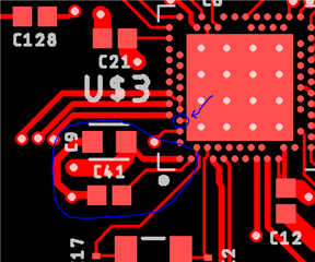
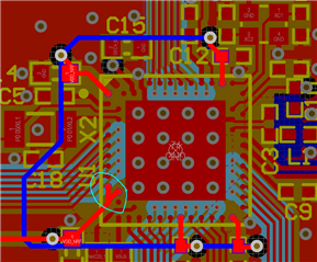
I've made my own PCB with an nrf52840. Right now I'm hoping to test out the bluetooth and measure my board's power consumption - the only problem is that I can't reliably program the microcontroller! A long time ago I was able to program this device with ble_app_blinky so I know the bluetooth works - unfortunately, right now I keep running into JLink errors. The specific setup/issues are listed below:

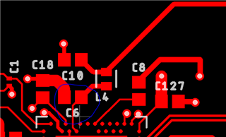
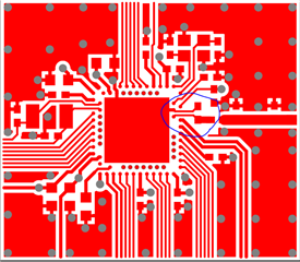
Right now I'm trying to program my custom board/NRF with 2 example projects: blinky and ble_app_blinky. To do so, I've setup the boards as in the diagram below:

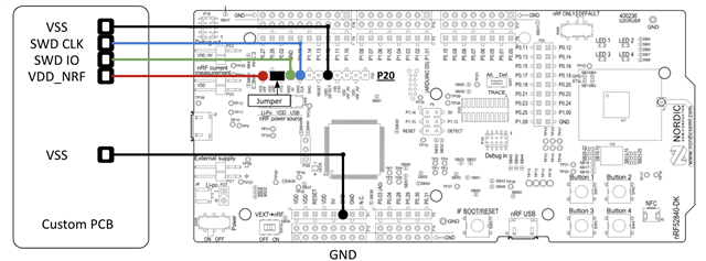
I am powering my custom board with an external supply set to 3.3V (the current limit is set to 3A so we should have more than enough juice) and the dev kit is "powered on" and plugged into my laptop via the uart/usb programming port (the left most usb port on the diagram). With this setup I can reliably program my custom board with the normal blinky program. Unfortunately, when I try to build&debug on my board with ble_app_blinky I get the following error:


Preparing target for download
Executing Reset script TargetInterface.resetAndStop()
Reset: Halt core after reset via DEMCR.VC_CORERESET.
Reset: Reset device via AIRCR.SYSRESETREQ.
Downloading ‘s140_nrf52_7.0.1_softdevice.hex’ to J-Link
Programming 2.7 KB of addresses 00000000 — 00000aff
Programming 149.3 KB of addresses 00001000 — 00026597
Failed to download application.
Error during program/erase phase.
Please check J-Link and target connection.
Download failed

sometimes when I "build & run" directly I get a slightly different error:

Reset: Halt core after reset via DEMCR.VC_CORERESET.
Reset: Reset device via AIRCR.SYSRESETREQ.
Downloading ‘s140_nrf52_7.0.1_softdevice.hex’ to J-Link
Programming 2.7 KB of addresses 00000000 — 00000aff
Programming 149.3 KB of addresses 00001000 — 00026597
J-Link: Flash download: Bank 0 @ 0x00000000: 2 ranges affected (4096 bytes)
J-Link: Flash download: Total: 0.652s (Prepare: 0.172s, Compare: 0.027s, Erase: 0.170s, Program & Verify: 0.106s, Restore: 0.175s)
J-Link: Flash download: Program & Verify speed: 37 KiB/s
Failed to download application.
Error during program/erase phase.
Please check J-Link and target connection.
Download failed

I'm using the latest version of the sdk (v17) and s140. To program my board I'm using SES. I have done all my development so far with the nrf52840 dk (PCA10056) and I figured I could use the same example files. Do I have to change the starting/stopping memory locations for programming? If not, does anyone have any suggestions for further log/debug steps I can proceed with?

I beseech the Nordic (company) gods.

Thank you,

Ryan

Parents
  • hen I try to build&debug on my board with ble_app_blinky I get the following error:

    looks like the board might be resetting during the session. 

    If you do not use the debug function does it work ?

    It is a vary strange cease, only ble_app_blinky?, could you test a --recover command to whip the chip? No other BLE samples have this issue?

    Regards,
    Jonathan

  • Hi Jonathan,

    Thanks for getting back to me!

    looks like the board might be resetting during the session. 

    I saw this vaguely mentioned in a few other posts but those situations seemed to be related to faulty USB ports, low voltages, or faulty connections. I can try another usb port today but I think I tried this out yesterday and it didn't change anything. Is there a flag I should toggle in SES?

    If you do not use the debug function does it work ?

    No, unfortunately. I usually get the same error - sometimes it looks different (the second code block), but it usually looks like the first error (first code block).

    It is a vary strange cease, only ble_app_blinky?, could you test a --recover command to whip the chip? No other BLE samples have this issue?

    I'm glad it's not just me! I can try other ble examples. Is it possible to use the "recover" command in SES? If so, how? hahaha. 

    Edit:

    I've tried out a few more examples, their results are listed below:

    1) simple_timer: works

    2) ble_beacon: Does NOT work - similar error

    3) ble_app_alert_notification: Does NOT work - similar error

    4) blinky_rtc_freeRTOS: Does NOT work - similar error

    So it seems that larger programs (that may/may not include soft device) cause it to break while programming. Right now the external board is drawing around 110 mA at 3.3V and the dev kit is connected to my macbook pro (with a USB-C to USB hub as an adaptor). If I try to power the external boards with 3V (which I thought I saw somewhere) it ends up bricking the chip (I keep getting "No idcode detected" which I guess is another problem).

    Also I've found the board that I know has a functioning NRF52840 & antenna so I can rule out any potential board manufacturing issues.

    Also thanks for your prompt response, Jonathan. I'm really lost and this is incredibly frustrating. I can't tell you how much I appreciate you helping me with this.

    Kindest regards,

    Ryan

  • Thanks for the update Ryan,

    Nice to see some progression!

    ryerye120 said:
    1) The interface wires are about 10cm actually. Should they be shorter?

    This is ok, 10cm should be fine, but long cables can introduce extra parasitic resistive and capacitive properties that might interfere, so to keep things predictable its good to have short cables.


    ryerye120 said:
    2) I'm still running at the default clock speed, I can reduce it if you think it will help the current problem.

    Lets keep this on hold for now.


    ryerye120 said:
    3) I've reduced the current limit to 100mA!

    Great!


    ryerye120 said:
    4) Yes, reducing the external supply to 3V results in a bricked chip. 

    This is interesting, but deserves its own ticket. 


    ryerye120 said:
    5) I will try nrf connect to erase/recover. Can I run nrf connect with the same setup?

    Yes, it is just a desktop app that you can easily use to test certain things and use features we develop for ease of use. 

    Connect the device to your computer, then launch the app and click on the select device button top right and select you device, you can then READ the device and it will show what i looks like, you can save this file for later to program the same device or other without building the code again, just use the hex file. 

    There are many options here, Read, Write, Erase, Erase and write and Reset. All  handy for testing and debugging. 


    ryerye120 said:
    6) No other HW problems that I know of right now.

    Good to know.


    ryerye120 said:
    7) I do have a dedicated crystal for my custom board's nrf52840. 

    This eliminates some potential issues, but i need to know it is the HFXO or LFXO, so do you have only one crystal or two ?


    ryerye120 said:
    8) After I bricked the chips I looked at VDD_nrf on the DK and it was at 3.3V I believe. I will double-check this to confirm (I should have double-checked this before I started messing with the external supply ... I guess I've learned the hard way.)

    You are not the first, guilty of this myself :D


    Now for the roadblock you have, we can continue discussing this here i think. I can do a review of the schematic and board layout files, see if i see any things that could be a issue. If you dont want to share design public i can make this ticket private, or you can just make a new ticket that is private and refer to this ticket in the new review ticket. 


    One thing i am interested in knowing is what do you gett if you Read the custom pcb device with nRF connect programmer app... this will show if it has been programmed correctly. 

    Regards,
    Jonathan

  • Hi Jonathan,


    Now for the roadblock you have, we can continue discussing this here i think. I can do a review of the schematic and board layout files, see if i see any things that could be a issue. If you dont want to share design public i can make this ticket private, or you can just make a new ticket that is private and refer to this ticket in the new review ticket. 

    I don't mind posting the schematics here!

    Firstly, when I plug my boards into the nrf connect programmer, I can only see the dev kit (that I'm using to program my custom board). Is there something specific I need to do to see the downstream microcontroller (the one on my custom PCB)?

    Secondly, while looking at other threads I came across this one describing a similar error but on a different chip. It turns out that when I comment out "idle_state_handle()" I can build & run!! Problem is ... well I don't know what the problem is normally. Why does idle_state_handle() break the code? I don't think it has anything to do with my custom PCB's power planes since I'm still just powering the custom board with the dev kit (which is connected to my computer with a usb cable).

    We're getting close! I can almost taste it.

    Kindest regards,

    Ryan

  • ryerye120 said:
    Firstly, when I plug my boards into the nrf connect programmer, I can only see the dev kit (that I'm using to program my custom board). Is there something specific I need to do to see the downstream microcontroller (the one on my custom PCB)?

    This is the expected behaviour, It is the debugger/programmer chip that is shown. 


    I dont quite see what could be the issue with idle_state_handle(), is it only for the ble_app_blinky you have tested this? any other changes you do to the applicaton?

    I think i will take a look at the HW and schematics first and then we can go from there. Can you provide them as PDF and if you have the HW files as GERBER that would be fantastic. 

    Regards,
    Jonathan

  • This is the expected behaviour, It is the debugger/programmer chip that is shown.

    I've only tested this with ble_app_blinky so far. I made 2 changes, 1 was commenting out idle_state_handle() and the other was to the pinout of LED4 (because that is different between the dev kit and my pcb). I will try another example! 

    I am working on getting the gerbers - in the meantime here are pdfs of the schematic and layout. This board is meant to test a custom IC that our research group designed, the nrf52840 is in the top left of the board.

    Thanks again for your help!!

    board_schematic.pdfboard_layout.pdf

  • So after looking at the schematic and layout pdf files, i have some comments, the layout you have does not exactly follow the recommendations we have for the nrf52840 and the deviations can\will effect at the very least RF performance. 

    There is enough space on the PCB that is should not be an issue to copy\paste the ref design on to the PCB. If you want i can provide more details on the layout of the nRF. But to keep things short it will mostly contain references to the ref design, best to have GERBER files to properly review and address the potential changes. 

    As for the cause of the issue you have now i dont think that it is HW related at the moment.

    Regards,
    Jonathan

Reply
  • So after looking at the schematic and layout pdf files, i have some comments, the layout you have does not exactly follow the recommendations we have for the nrf52840 and the deviations can\will effect at the very least RF performance. 

    There is enough space on the PCB that is should not be an issue to copy\paste the ref design on to the PCB. If you want i can provide more details on the layout of the nRF. But to keep things short it will mostly contain references to the ref design, best to have GERBER files to properly review and address the potential changes. 

    As for the cause of the issue you have now i dont think that it is HW related at the moment.

    Regards,
    Jonathan

Children
  • Hi Jonathan,

    Thank you for looking at the schematic and design! It's been a while since I did the schematic/layout but I think we were trying to stay as close as possible to the CKAA WLCSP schematic #3 with a few changes to the antenna (we wanted to use a dedicated antenna chip). Here are the appropriate gerbers (I think). I would really appreciate any feedback!

    gerbers.zip

    As for other examples I have tested ble_app_alert_notification and ble_app_beacon and both exhibited the same behavior as blinky. Worked the first time with build & debug. If I power cycled the board or did a "build & run" they board would halt. If I commented out "nrf_power_mgmt_run()" things work as expected.

    As always, thank you for your help,

    Ryan

  • Hi Ryan, 

    Looking at the files there are some tings i want to comment on.

    1. it would be good to have a top layer ground pour. More ground surface area does help reduce return paths and can be used to create coplanar wave guides in sted of strip lines. We do recommend the grounded coplanar wave guide as we have seen that they often preform better.

    2. The decupling cap on the first radio matching component is not directly following the ref. design.  We do have some notes that point to the fact that it is not just matching but also filering of the harmonics so it is best to keep the layout identical. You do have more then enough space to do a copy past of the design. 


    3. Since there is no top layer ground you are also missing out on the some of the pinns that benefit from being connected to top layer ground might give reduced radio performance. The decupling caps here help filter the supply so that no as lite noise as possible can get to the radio.


    ryerye120 said:
    close as possible to the CKAA WLCSP schematic #3

    Did you mean QIAA  no. 3?  aQFN package, in your design that is what is used at least. 


    But i think the layout is ok, adding top layer ground would solve many of the "issues", choice of antenna is good also, many use it and it preforms well.


    As for the application halting after reset issue, i have not figured this out, so will update in a day or two to wit more info\debugging options you can test. Sorry for the slow response.  

    Regards,
    Jonathan

  • Hi Jonathan,

    Did you mean QIAA  no. 3?  aQFN package, in your design that is what is used at least. 

    Sorry, you're right. We're using the aQFN packaged chips. The most important point was that we are powering the chip with an external regulator & originally wanted to have the USB interface (but I'm pretty sure we ended up scraping that and just left the USB interface pulled up/down - whatever it needed to be)

    But i think the layout is ok, adding top layer ground would solve many of the "issues", choice of antenna is good also, many use it and it preforms well.

    We'll definitely incorporate this in our next board!! Thank you for the suggestion.

    As for the application halting after reset issue, i have not figured this out, so will update in a day or two to wit more info\debugging options you can test. Sorry for the slow response.  

    No worries, I figure it is a weird bug. Could it be related to how we've wired VDD and VDDH? I'm wondering if I missed a power connection.

  • Hi Ryan, here is the ref design, and compared to yours it does not differ that much, so i dont think it is the issue. 

    So does not look like you have a missed power connection. 


    Maybe try a different SDK version or different SDK? see if the behaviour is still the same. And have you tested on more then one custom board?

    Regards,
    Jonathan

  • Hi Jonathan,

    I've tried multiple boards and they all have this issue. We even re-spun the boards (for other reasons) and the re-spun boards have the same issue.

    I've tried it with SDK 16 and it had the same issue.

    Is there a reference design Eagle Project that I could maybe get access to? If so, maybe I can just plop that directly into our design?

    Kindest regards,

    Ryan

Related